DS586PP5
81
CS42528
12.1
External Filter Components
12.1.1
General
The PLL behavior is affected by the external filter component values in the Typical Connection Diagrams.
Figure 5 show the recommended configuration of the two capacitors and one resistor that comprise the
PLL filter. The external PLL component values listed in Table 21 have a high corner frequency jitter atten-
uation curve, take a short time to lock, and offer good output jitter performance. Lock times are worst case
for an Fsi transition of 192 kHz.
It is important to treat the LPFILT pin as a low level analog input. It is suggested that the ground end of
the PLL filter be returned directly to the AGND pin independently of the digital ground plane.
It should be noted that, for backward compatibility with Revision C, these components may be used with
Revision D silicon with the LOCKM (register 24h, bit 6) set to ‘0’.
12.1.2
Jitter Attenuation
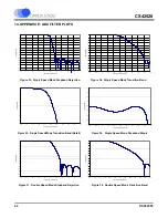
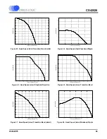
Shown in Figure 28 is the jitter attenuation plot when used with the external PLL component values listed
in Table 21 for the 32-192 kHz Fs Range. The AES3 and IEC60958-4 specifications do not have allow-
ances for locking to sample rates less than 32 kHz or for locking to the SAI_LRCK input. These specifica-
tions state a maximum of 2 dB jitter gain or peaking.
RFILT (k
Ω
) CFILT (
µ
F) CRIP (pF)
2.55
0.047
2200
Table 21. PLL External Component Values
Figure 28. Jitter Attenuation Characteristics of PLL

