CDB43198-GBK
DS1156DB1
5
2 CDB43198 Board Overview
The CDB43198 is the board for evaluating the performance of the CS43198. It supports multiple power supplies and
signal I/O configurations.
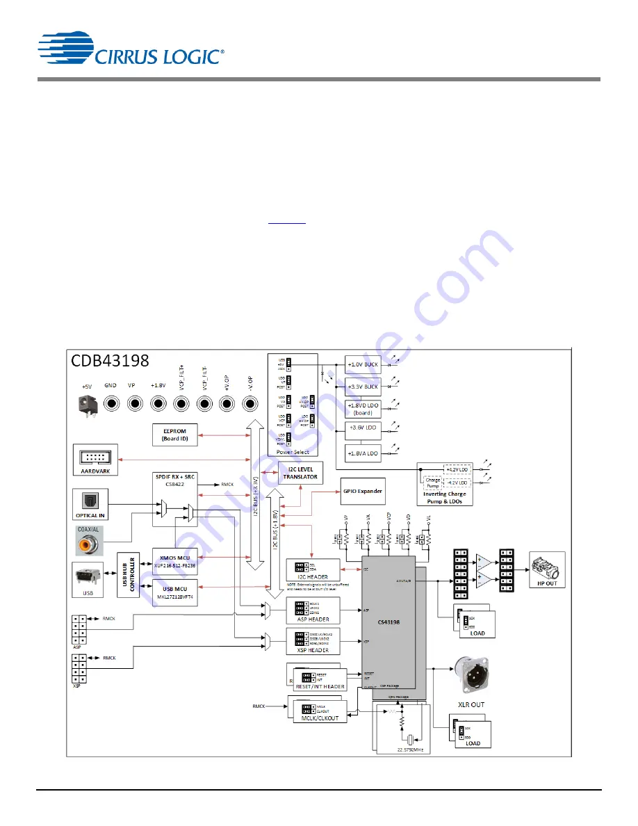
The CDB43198 board uses five buffers with direction control to direct clock from the digital input sources to/from the
CS43198 DUTs. Two buffers, the PCM/DoP buffer and the DSD/DoP buffer, support voltage translation from 3.3 V to 1.8
V and vice versa. The voltage selection is done through headers: J28 for the PCM/DoP buffer and the DSD/DoP buffer.
The S/PDIF buffer is a unidirectional buffer and supports 3.3 V to 1.8 V translation. The remaining buffers only support 1.8
V signals. These buffers are controlled by an I/O Expander. The I/O Expander can be controlled through its I
2
C interface.
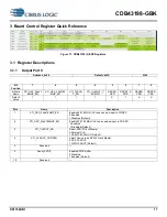
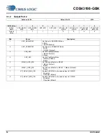
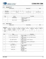
The register map for I/O Expander is described in
Section
3. The direction of clock signals is determined by the
CS43198’s operating mode (master or slave mode).
The CDB43198 can also communicate with a smart codec through the use of J42. The purpose of using a smart codec is
to allow the user to perform listening tests with various equalizer (EQ) filters based on the impedance of the attached
headphone. The CDB43198 board allows the PCM input to be routed to the smart codec. The codec can then apply an
EQ filter on this data, based on the impedance of the attached headphone and send EQ-filtered data to the CS43198, for
an optimal listening experience. The following diagram shows an overview of the CDB43198 board.
Since the CDB43198 does not have an integrated headphone driver, there is an OPA1622 High-Fidelity Audio Amplifier
on the output of the CSP device, which is able to drive headphone type loads.
Figure 4 CDB43198 Block Diagram


