42
©
Copyright 2004 Cirrus Logic, Inc.
DS651UM21
Version 2.1
CobraNet Hardware User’s Manual
Mechanical Drawings and Schematics
9.2
CM-2 Schematics
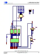
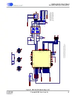
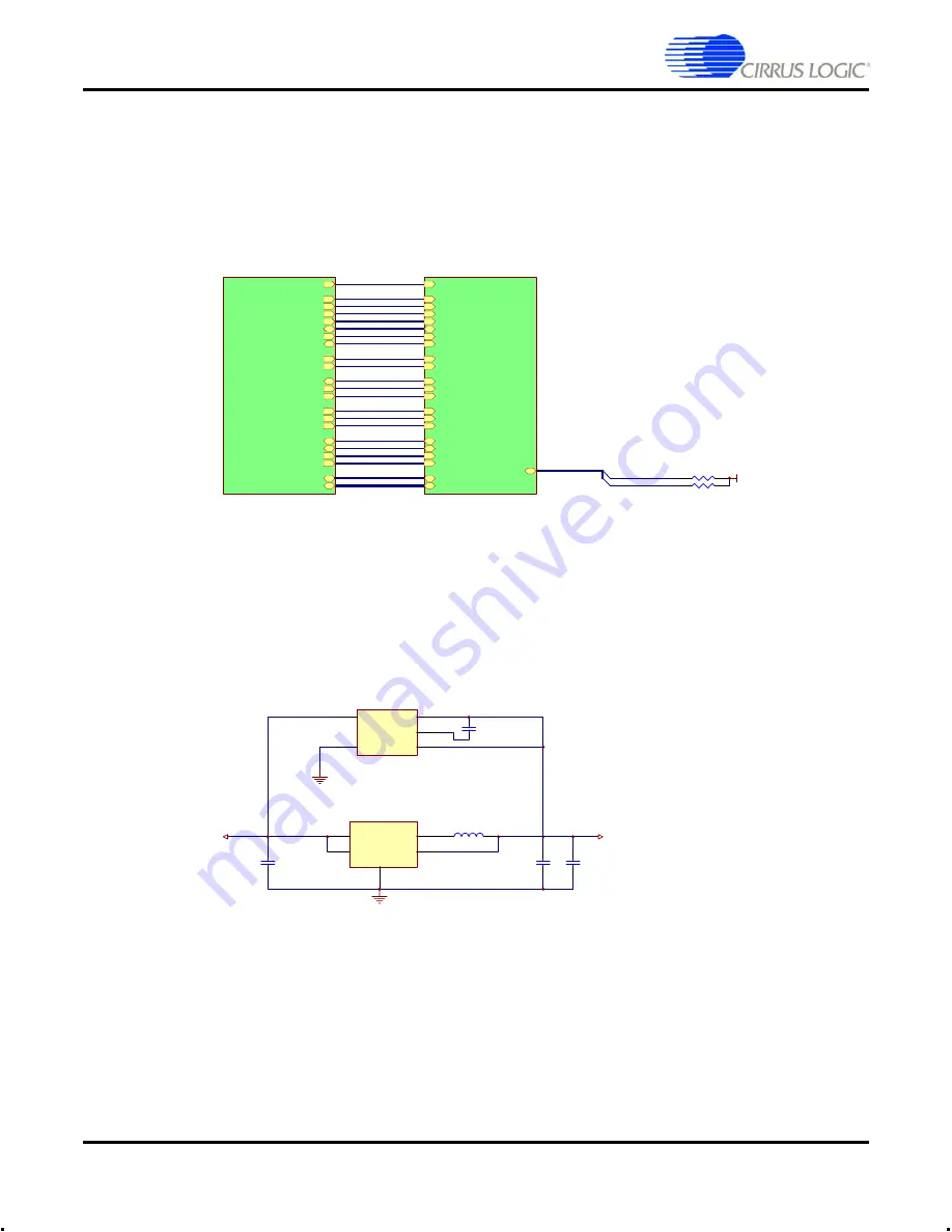
Figure 22. CM-2 RevE Schematic Page 1 of 7
RUN
1
GND
2
SW
3
VIN
4
Vout/FB
5
U1
LTC3406-1.8
VCC_+3.3
L1
2.2 uH
VCC_+1.8
C2
10 uF, X5R, 6.3 Volts
C1
10 uF, X5R, 6.3 Volts
C3
This is a simple switching regulator. It produces
1.8V at >500 mA at about 90% efficency. A simple low drop
out linear regulator would be a cheaper alternative at the
expense of power. A linear regulator would dissapate
about 0.75 watts max, This switching regulator dissapates
about 0.10 watts max.
HRESET#
HEN#
HRW
HDS#
HADDR[0..3]
HDATA[0..7]
HREQ#
HACK#
WATCHDOG
MUTE#
UART_TX_OE
UART_TXD
UART_RXD
MCLK_OUT
MCLK_IN
REFCLK_IN
FS1
SSI_CLK
SSI_DIN[0..3]
SSI_DOUT[0..3]
AUX_POWER[0..3]
GPIO[0..1]
R2
10K Ohm
R1
GPIO0
GPIO1
GND
GPIO[0..1] is not used elsewhere.
These pulldowns are used for test points and
to keep these signals at valid levels.
IN
1
GND
2
BYP
3
OUT
4
ADJ
5
U9
LTC1761
C45
0.01 uF
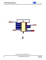
This linear regulator is used to assure that the +1.8v rail quickly passes
the 0.5v threshold at powerup, thus minimizing power sequencing issues
and making sure that the DSP does not draw excessive power as the
power rails ramp up. This linear regulator is set with Vout=1.22v, so it
is effectively shut off once the switching regulator comes up. Further
testing and characterization of the DSP is require to determine if this
linear regulator is in fact required.
HRESET#
HACK#
HDATA[0..7]
HADDR[0..3]
HRW
HDS#
HEN#
HREQ#
SSI_DOUT[0..3]
SSI_DIN[0..3]
SSI_CLK
MCLK_OUT
FS1
UART_TXD
UART_RXD
MCLK_IN
REFCLK_IN
UART_TX_OE
AUX_POWER[0..3]
WATCHDOG
MUTE#
RSVD[1..5]
connector
connector.sch
AUX_POWER[3..0]
UART_TX_OE
UART_RXD
UART_TXD
HRW
HDS#
HEN#
HREQ#
HACK#
HADDR[0..3]
HDATA[0..7]
FS1
SSI_CLK
SSI_DOUT[0..3]
SSI_DIN[0..3]
GPIO[0..1]
HRESET#
REFCLK_IN
WATCHDOG
MUTE#
MCLK_IN
MCLK_OUT
RSVD[1..5]
core
core.sch
RSVD[1..5]


