background image

CobraNet Hardware User’s Manual

Digital Audio Interface 

DS651UM21

©

Copyright 2004 Cirrus Logic, Inc.

19

Version 2.1

6.0 Digital Audio Interface 

The CS18101, CS18102, and CM-2 support four bi-directional synchronous serial 
interfaces. The CS18100 supports one bi-directional synchronous serial interface. All 
interfaces operate in master mode with DAO1_SCLK as the bit clock and FS1 as the 
frame clock. A sample period worth of synchronous serial data includes two (or four) 
audio channels. CobraNet supports two synchronous serial bit rates: 48 Khz and 96 KHz. 
However, 96 kHz sample rate is not available when using CS18102 with 16X16 channels. 
Bit rate is selected by the 

modeRateControl

 variable. All synchronous serial interfaces 

operate from a common clock at the same bit rate.

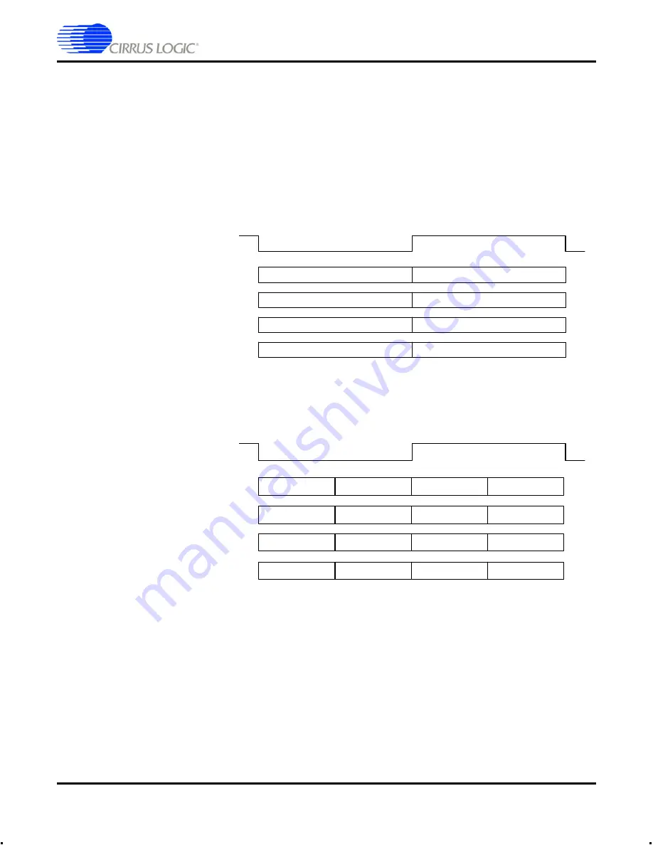
Figure 4.  Channel Structure for Synchronous Serial Audio at 64FS (One Sample Period) - CS18100 & CS18101

Figure 5.  Channel Structure for Synchronous Serial Audio at 128FS (One Sample Period) - CS18102

Default channel ordering is shown above. Note that the first channel always begins after 
the rising or falling edge of FS1 (depending on the mode). 

DAI1_SCLK period depends on the sample rate selected. Up to 32 significant bits are 
received and buffered by the DSP for synchronous inputs. Up to 32 significant bits are 
transmitted by the DSP for synchronous outputs. Bit 31 is always the most significant 
(sign) bit. A 16-bit audio source must drive to bit periods 31-16 with audio data and bits 
15-0 should be actively driven with either a dither signal or zeros. Cirrus Logic 
recommends driving unused LS bits to zero. 


1

2  

F S 1  

D A O 1 _ D A T A 0  / D A I1 _ D A T A 0  

3

4  

5

6  

7

8  

*D A O 1 _ D A T A 1  / D A I1 _ D A T A 1  

*D A O 1 _ D A T A 2  / D A I1 _ D A T A 2  

*D A O 1 _ D A T A 3  / D A I1 _ D A T A 3  

* N o t p re s e n t  in   C S 1 8 1 0 0 . 


1

2

FS1 

DAO1_DATA0 / DAI1_DATA0 

5

6

9

10

13

14

DAO1_DATA1 / DAI1_DATA1 

DAO1_DATA2 / DAI1_DATA2 

DAO1_DATA3 / DAI1_DATA3 

3

4

7

8

11

12

15

16


Summary of Contents for CobraNet CM-2

Page 1: ...g Processor CS181xx Preliminary Product Information This document contains information for a new product Cirrus Logic reserves the right to modify this product without notice CobraNet S i l i c o n S e r i e s CS18100 CS18101 CS18102 and CM 2 Hardware User s Manual Version 2 1 Replaces DS651UM20 ...

Page 2: ...2 Copyright 2004 Cirrus Logic Inc DS651UM21 CobraNet Hardware User s Manual 32 bit Audio Decoder DSP Family NOTES ...

Page 3: ...gnals 14 4 2 6 Power and Ground Signals 14 4 2 7 System Signals 15 5 0 Synchronization 16 5 1 Synchronization Modes 16 5 1 1 Internal Mode 17 5 1 2 Internal Mode with External Sample Synchronization 17 5 1 3 External Word Clock Mode 17 5 1 4 External Master Clock Mode 18 5 1 5 External Master Clock Mode with External Sample Synchronization 18 6 0 Digital Audio Interface 19 6 1 Digital Audio Interf...

Page 4: ... Timing Overview 20 Figure 8 Audio Data Timing Detail Normal Mode 64FS CS18100 CS18101 21 Figure 9 Audio Data Timing Detail Normal Mode 128FS CS18102 21 Figure 10 Audio Data Timing Detail I2S Mode 64FS CS18100 CS18101 21 Figure 11 Audio Data Timing Detail I2S Mode 128FS CS18102 21 Figure 12 Audio Data Timing Detail Standard Mode 64FS CS18100 CS18101 22 Figure 13 Audio Data Timing Detail Standard M...

Page 5: ...aNet interface performs synchronous to isochronous and isochronous to synchronous conversions as well as the data formatting required for transporting real time digital audio over the network The CobraNet interface has provisions for carrying and utilizing control and monitoring data such as Simple Network Management Protocol SNMP through the same network connection as the audio Standard data tran...

Page 6: ...ties Reduced cost Improved performance Convergent Audio Distribution Infrastructure 2 2 CobraNet Interface Auto negotiating 100Mbit Full duplex Ethernet Connections 16 channel Audio I O Capability Implements CobraNet Protocol for real time transport of audio over Ethernet Local Management via 8 bit Parallel Host Port UDP IP Network Stack with Dynamic IP Address Assignment via BOOTP or RARP Remote ...

Page 7: ...00 and CS18101 128FS 6 144 MHz Bit Rate for CS18102 Accommodates Many Synchronous Serial Formats Including I2 S 32 bit Data Resolution on All Audio I O 2 6 Audio Clock Interface 5 Host Audio clocking Modes for Maximum Flexibility in Digital Audio Interface Design Low jitter Master Audio Clock Oscillator 24 576 MHz Synchronize to Supplied Master and or Sample Clock Sophisticated jitter attenuation ...

Page 8: ...ronous to isochronous and isochronous to synchronous conversions The CS181xx has a role in sample clock regeneration and performs all interactions with the host system The sample clock is generated by a voltage controlled crystal oscillator VCXO controlled by the CS181xx The VCXO frequency is carefully adjusted to achieve lock with the network clock The Ethernet controller is a standard interface ...

Page 9: ...ils the chip pinout and signal interfaces for each module and is divided as follows CS181xx Package Pinouts on page 10 Host Port Signals on page 12 Asynchronous Serial Port UART Bridge Signals on page 12 Synchronous Serial Audio Signals on page 13 Audio Clock Signals on page 13 Miscellaneous Signals on page 14 Power and Ground Signals on page 14 System Signals on page 15 ...

Page 10: ...DDD 12 NC 48 DATA9 84 ADDR16 120 HDATA1 13 GND 49 DATA8 85 ADDR17 121 HDATA0 14 DAO2_LRCLK 50 NC 86 GND 122 GND 15 DAO1_DATA3 51 NC 87 ADDR18 123 XTAL_OUT 16 DAO1_DATA2 HS2 52 NC 88 ADDR19 124 XTO 17 DAO1_DATA1 HS1 53 NC 89 OE 125 XTI 18 VDDIO 54 VDDD 90 CS1 126 GND_a 19 DAO1_DATA0 HS0 55 ADDR12 91 VDDIO 127 FILT2 20 DAO1_SCLK 56 ADDR11 92 MUTE 128 FILT1 21 GND 57 GND 93 HRESET 129 VDD_A 22 DAO1_L...

Page 11: ... 3V J1 J2 A9 HADDR1 J1 J2 B16 GND J3 J4 B3 GND J1 J2 A10 HADDR2 J1 J2 B17 VCC_ 3 3V J3 J4 B4 VCC_ 3 3V J1 J2 A11 HDATA0 J1 J2 B18 RSVD1 J3 J4 B5 GND J1 J2 A12 HDATA1 J1 J2 B19 GND J3 J4 B6 VCC_ 3 3V J1 J2 A13 HDATA2 J1 J2 B20 VCC_ 3 3V J3 J4 B7 GND J1 J2 A14 HDATA3 J3 J4 A1 RSVD2 J3 J4 B8 VCC_ 3 3V J1 J2 A15 HDATA4 J3 J4 A2 MUTE J3 J4 B9 GND J1 J2 A16 HDATA5 J3 J4 A3 FS1 J3 J4 B10 VCC_ 3 3V J1 J2 ...

Page 12: ...x Pin Notes HDATA 7 0 Host Data In Out J1 A19 A 17 11 111 112 114 115 117 118 102 121 Host port data HADDR 3 0 Host Address In J1 A20 A 10 8 105 106 109 110 Host port address HRW Host Direction In J1 A4 107 Host port transfer direction HREQ Host Request Out J1 A6 140 Host port data request HACK Host Alert Out J1 A3 102 Host port interrupt request HDS Host Strobe In J1 A5 103 Host port strobe HEN H...

Page 13: ...7 19 Output synchronous serial audio data DAO1_DATA 3 1 not used for CS18100 DAI1_DATA 3 0 Audio Input Data In J3 A 15 12 131 132 134 135 Input synchronous serial audio data DAI1_DATA 3 1 not used for CS18100 DAI1_SCLK Audio Bit Clock In J4 A7 137 Should be tied to DAO1_SCLK Synchronous serial bit clock Signal Description Direction CM 2 Pin CS181xx Pin Notes DAI1_LRCLK Sample clock input In 138 Sh...

Page 14: ...t improper operation can also be indicated by short pulses 100 ns MUTE Interface Ready Out J3 A2 92 Asserts active low during initialization and when a fault is detected or connection to the network is lost NC No Connect 28 50 53 78 81 141 142 Signal Description CM 2 Pin CS181xx Pin Specification VCC_ 3V System Digital 3 3 v J1 B20 B17 B15 B13 B11 B9 B7 B5 B3 J3 B14 B12 B10 B8 B6 B4 B2 N A 3 3 0 3...

Page 15: ...ed for normal operation 9 DATA 15 0 Data Bus for Flash Ethernet Controller s 29 32 34 35 37 39 43 45 46 48 49 ADDR 19 0 Address Bus for Flash Ethernet Controller s 55 56 58 59 61 62 64 67 68 70 72 74 75 77 82 84 85 87 88 WE Write Enable for Flash and Ethernet Controller s 38 CS1 Chip Select for Flash Memory Device 90 CS2 Chip Select for Ethernet Controller s 65 OE Output Enable 89 IOWAIT Wait Stat...

Page 16: ...rformerClock The role conductor or performer is determined by the network environment including the conductor priority setting of the device and the other devices on the network It is possible to ensure you will never assume the conductor role by selecting a conductor priority of zero However it is not reasonable to assume that by setting a high conductor priority you will always assume the conduc...

Page 17: ...ice that already has circuitry for generating those clocks Conductor The VCXO is parked according to the syncClockTrim setting Performer The VCXO is steered to match the clock transmitted by the conductor 5 1 3 External Word Clock Mode All CobraNet clocks are derived from the onboard VCXO The VCXO is steered from an external clock supplied to the reference clock input The clock supplied can be any...

Page 18: ...ally lock to the network clock and will jam sync via the supplied master clock The external clock source must be synchronous with the network conductor 5 1 5 External Master Clock Mode with External Sample Synchronization This mode is identical to External Master Clock mode except that it allows synchronization of the derived clocks sample clock audio bit clock to an external source via the refere...

Page 19: ...ne Sample Period CS18100 CS18101 Figure 5 Channel Structure for Synchronous Serial Audio at 128FS One Sample Period CS18102 Default channel ordering is shown above Note that the first channel always begins after the rising or falling edge of FS1 depending on the mode DAI1_SCLK period depends on the sample rate selected Up to 32 significant bits are received and buffered by the DSP for synchronous ...

Page 20: ...ng Relationship between FS512_OUT DAO1_SCLK and FS1 An DAO1_SCLK edge follows an MCLK_OUT edge by 0 0 to 5 0ns An FS1 edge follows a MCLK_OUT edge by 0 0 to 10 0ns Note The DAO1_SCLK and FS1 might be synchronized with the either the falling edge or the rising edge of MCLK_OUT Which edge is impossible to predict since it depends on power up timing Figure 7 Serial Port Data Timing Overview Setup tim...

Page 21: ...a is sampled on the rising edge of DAI_SCLK and data changes on the falling edge FS1 DAI1_DATAx DAO1_DATAx DAI1_SCLK 23 22 21 20 19 18 17 16 15 14 13 12 11 10 9 8 7 6 5 4 3 2 23 1 0 Unused 23 22 21 20 19 18 17 16 15 14 13 12 11 10 9 8 7 6 5 4 3 2 23 1 0 Unused FS1 DAI1_DATAx DAO1_DATAx DAI1_SCLK 23 22 21 20 19 18 17 16 15 14 13 12 11 10 9 8 7 6 5 4 3 2 23 1 0 Unused 22 21 20 19 18 17 16 15 14 13 1...

Page 22: ...t justified and is aligned with FS1 Data is sampled on the rising edge of DAI_SCLK and data changes on the falling edge FS1 DAI1_DATAx DAO1_DATAx DAI1_SCLK 23 22 21 20 19 18 17 16 15 14 13 12 11 10 9 8 7 6 5 4 3 2 23 1 0 Unused 23 22 21 20 19 18 17 16 15 14 13 12 11 10 9 8 7 6 5 4 3 2 23 1 0 Unused FS1 DAI1_DATAx DAO1_DATAx DAI1_SCLK 23 22 21 20 19 18 17 16 15 14 13 12 11 10 9 8 7 6 5 4 3 2 23 1 0...

Page 23: ... Definitions on page 31 and HMI Access Code on page 32 Table 3 Host port memory map The message and data registers provide separate bi directional data conduits between the host processor and the CS181xx A 32 bit word of data is transferred to the CS181xx when the host writes the D message or data register after presumably previously writing the A B and C registers with valid data Data is transfer...

Page 24: ...aking on the HREQ pin bit should be observed to prevent overflowing the input data buffer Parameter Symbol Min Max Unit Address setup before HEN and HDS low tmas 5 ns Address hold time after HEN and HDS low tmah 5 ns Read Delay between HDS then HEN low or HEN then HDS low tmcdr 0 ns Data valid after HEN and HDS low with HR W high tmdd 19 ns HEN and HDS low for read tmrpw 24 ns Data hold time after...

Page 25: ...rt Read Cycle Timing Figure 15 Host Port Write Cycle Timing t mas t mcdr tm ah t mdd t m rpw t mdhr t mdis tm rd t mrdtw t mrwsu t m rw hld HADDR 3 0 HDATA 7 0 HEN HR W HDS HREQ tmrwirqh LSP MSP t m as t m dsu t m dhw t m w d t m w trd t m w pw t m cdw t m rw su t m rw hld m ah t HADDR 3 0 HDATA 7 0 HEN HR W HDS HREQ tm rwirql LSP M SP ...

Page 26: ...ites to the A B and C registers Writing to the D register transmits the message to the CS181xx A listing of all HMI messages is shown in Table 4 Refer also to HMI Definitions on page 31 and HMI Access Code on page 32 Table 4 HMI messages Message DRQ Handshake Mode A B C D Translate Address n c Address MS Address Address LS 0xB3 Acknowledge Interrupt n c n c n c n c 0xB4 Identify read n c n c 7 0xB...

Page 27: ...SG_D CVR_TRANSLATE_ADDRESS while msgack MSG_D 1 MSG_TOGGLE_BO 7 3 1 2 Interrupt Acknowledge Causes HACK to be de asserted void InterruptAck void int msgack MSG_D MSG_D CVR_INTERRUPT_ACK while msgack MSG_D 1 MSG_TOGGLE_BO 7 3 1 3 Goto Packet Moves HMI pointers to bridgeRxPktBuffer write 0 or bridgeTxPktBuffer write 1 void GotoPacket bool write int msgack MSG_D MSG_C write MOP_GOTO_PACKET_TRANSMIT M...

Page 28: ...E_BO 7 3 1 6 Packet Transmit Sets bridgeTxPkt bridgeTxPktDone 1 thus initiating transmission of the contents of bridgeTxPktBuffer Presumably bridgeTxPktBuffer has been previously written with valid packet data void PacketTransmit void int msgack MSG_D MSG_C MOP_PACKET_TRANSMIT MSG_D CVR_MULTIPLEX_OP while msgack MSG_D 1 MSG_TOGGLE_BO 7 3 1 7 Goto Counters Moves HMI data pointers to interrupt statu...

Page 29: ... is read Reading the message conduit gives the current status as of the last time the D register of the conduit was read Bitfields in the HMI Status Register are outlined in Table 5 below Refer also to HMI Definitions on page 31 and HMI Access Code on page 32 Table 5 HMI status bits Status Bit s Reserved 31 24 Region Length 23 8 Reserved 7 5 Writable Region 4 Translation Complete 3 Packet Transmis...

Page 30: ...sults are available and a new translation request may be submitted This bit is cleared when a Translate Address message is issued and is set when the translation completes 7 3 3 4 Packet Transmission Complete This bit is cleared when transmission is initiated by issuance of the Transmit Packet message The bit is set when the packet has been transmitted and the transmit buffer is ready to accept a ...

Page 31: ...define DATA_B 5 define DATA_C 6 define DATA_D 7 define CONTROL 8 define STATUS 9 define CVR_SET_ADDRESS 0xb2 Not availbale on CS181xx CM 2 CM 1 and Reference Design only define CVR_TRANSLATE_ADDRESS 0xb3 define CVR_INTERRUPT_ACK 0xb4 define CVR_MULTIPLEX_OP 0xb5 define MOP_GOTO_TRANSLATION_READ 0 define MOP_GOTO_TRANSLATION_WRITE 5 define MOP_GOTO_PACKET_RECEIVE 1 define MOP_GOTO_PACKET_TRANSMIT 6...

Page 32: ...ReadRegister int hmiregister return unsigned char volatile const hmiregister HMI_BASE void WriteRegister int hmiregister unsigned char value unsigned char volatile const hmiregister HMI_BASE value void SendMessage unsigned char message int msgack ReadRegister MSG_D issue last byte of message WriteRegister MSG_D message wait for acceptance of message while msgack ReadRegister MSG_D 1 MSG_TOGGLE_BO ...

Page 33: ...long Peek long address if address PeekPointer SetAddress address if PeekPointer PeekLimit throw Peek addressing error unsigned long value ReadRegister DATA_A 24 value ReadRegister DATA_B 16 value ReadRegister DATA_C 8 value ReadRegister DATA_D PeekPointer maintain local pointer return value void Poke long address unsigned long value if address PokePointer SetAddress address if PokePointer PokeLimi...

Page 34: ...r to flip data bus if MSG_B 0x55 read back CVR redo same detection with different data MSG_B 0x3c DATA_A 0xc3 if MSG_B 0x3c return 1 CM 1 detected check for presence of CM 2 issue identify command MSG_C MOP_IDENTIFY MSG_D CVR_MULTIPLEX_OP int msgack MSG_D clean pipeline msgack MSG_D wait for togglebit to flip in response to command int tm0 gettimeofday while MSG_D toggle 1 MSG_TOGGLE_BO int tm1 ge...

Page 35: ...n page 36 General PCB Dimensions on page 37 Example Configuration Side View on page 38 Faceplate Dimensions on page 39 Case Cutout for Faceplate Mounting on page 40 Connector Detail on page 41 CM 2 RevE Schematic Page 1 of 7 on page 42 CM 2 RevE Schematic Page 2 of 7 on page 43 CM 2 RevE Schematic Page 3 of 7 on page 44 CM 2 RevE Schematic Page 4 of 7 on page 45 CM 2 RevE Schematic Page 5 of 7 on ...

Page 36: ...us Logic Inc DS651UM21 Version 2 1 CobraNet Hardware User s Manual Mechanical Drawings and Schematics 9 1 CM 2 Mechanical Drawings Figure 16 CM 2 Module Assembly Drawing J3 J1 Flash CS181xx DM9000 DM9000 U7 U8 U6 T1 U5 J5 J6 ...

Page 37: ...CobraNet Hardware User s Manual Mechanical Drawings and Schematics DS651UM21 Copyright 2004 Cirrus Logic Inc 37 Version 2 1 Figure 17 General PCB Dimensions ...

Page 38: ...38 Copyright 2004 Cirrus Logic Inc DS651UM21 Version 2 1 CobraNet Hardware User s Manual Mechanical Drawings and Schematics Figure 18 Example Configuration Side View ...

Page 39: ...CobraNet Hardware User s Manual Mechanical Drawings and Schematics DS651UM21 Copyright 2004 Cirrus Logic Inc 39 Version 2 1 Figure 19 Faceplate Dimensions ...

Page 40: ...40 Copyright 2004 Cirrus Logic Inc DS651UM21 Version 2 1 CobraNet Hardware User s Manual Mechanical Drawings and Schematics Figure 20 Case Cutout for Faceplate Mounting Required Panel Cutout ...

Page 41: ...CobraNet Hardware User s Manual Mechanical Drawings and Schematics DS651UM21 Copyright 2004 Cirrus Logic Inc 41 Version 2 1 Figure 21 Connector Detail J3 J1 Component Side Up ...

Page 42: ...not used elsewhere These pulldowns are used for test points and to keep these signals at valid levels IN 1 GND 2 BYP 3 OUT 4 ADJ 5 U9 LTC1761 C45 0 01 uF This linear regulator is used to assure that the 1 8v rail quickly passes the 0 5v threshold at powerup thus minimizing power sequencing issues and making sure that the DSP does not draw excessive power as the power rails ramp up This linear regu...

Page 43: ... LED_BUF1 LED_BUF2 LED_BUF3 LED_BUF4 LED_BUF5 LED_BUF6 LED_BUF7 LED_BUF 0 7 LED_CTRL 0 2 LED_CTRL0 LED_CTRL1 LED_CTRL2 GND VCC_ 3 3 VCC_ 3 3 LED_CTRL 0 2 LED_BUF 0 7 LED_BUF 0 7 MCLK_IN VCXO_OUT VCXO_OUT VCXO_OUT GND GND GND GND MCLK_INTERNAL MCLK_OUT R16 24 9 Ohm 1 VCC_ 3 3 C19 0 1 uF R12 3 3K Ohm VCXO_CTRL MCLK_IN VCXO_CTRL MCLK_SEL MCLK_INTERNAL MCLK_OUT C21 0 1 uF VCC_ 3 3 C22 0 1 uF VCC_ 3 3 ...

Page 44: ...1 A3 22 A2 23 A1 24 A0 25 CE 26 GND 27 OE 28 D0 29 D8 30 D1 31 D9 32 D2 33 D10 34 D3 35 D11 36 VCC 37 D4 38 D12 39 D5 40 D13 41 D6 42 D14 43 D7 44 D15 A 1 45 GND 46 BYTE 47 A16 48 U5 FLASH_TSOP VCC_ 3 3 ADDR0 ADDR1 ADDR2 ADDR3 ADDR4 ADDR5 ADDR6 ADDR7 ADDR8 ADDR9 ADDR10 ADDR11 ADDR12 ADDR13 ADDR14 ADDR15 ADDR16 ADDR17 ADDR18 ADDR19 ADDR 0 19 DATA 0 15 DATA 0 15 ADDR 0 19 HRESET_BUF HRESET_BUF OE WE...

Page 45: ...D1 48 SD_D8 EXT_D0 49 U6 CS18101 VCC_ 1 8 VCC_ 3 3 HRESET_BUF OE WE FLASH_CS MAC_CS IOWAIT DATA0 DATA1 DATA2 DATA3 DATA4 DATA5 DATA6 DATA7 DATA8 DATA9 DATA10 DATA11 DATA12 DATA13 DATA14 DATA15 ADDR0 ADDR1 ADDR2 ADDR3 ADDR4 ADDR5 ADDR6 ADDR7 ADDR8 ADDR9 ADDR10 ADDR11 ADDR12 ADDR13 ADDR14 ADDR15 ADDR16 ADDR17 ADDR18 ADDR19 UART_TXD UART_RXD UART_TX_OE HDATA0 HDATA1 HDATA2 HDATA3 HDATA4 HDATA5 HDATA6...

Page 46: ... 15 HRESET_BUF VCC_ 3 3 GND OE WE MAC_CS IOWAIT HRESET_BUF OE WE MAC_CS IOWAIT MAC_IRQ0 MAC_IRQ0 ADDR2 ADDR3 ADDR1 ADDR4 LED_CTRL 0 2 LED_CTRL 0 2 VCC_ 3 3 VCC_PHY1 C46 0 01 uF FB2 FBEAD 68 Ohm 100 MHz C6 10 uF X5R 6 3 Volts C7 10 uF X5R 6 3 Volts VCC_ 3 3 VCC_PHY1 1 2 3 4 5 6 7 8 CN8 0 1 uF 4x Array 1 2 3 4 5 6 7 8 CN6 0 1 uF 4x Array VCC_ 3 3 1 2 3 4 5 6 7 8 CN7 0 1 uF 4x Array GND 1 2 3 4 5 6 7...

Page 47: ...ing Failure to properly install and configure the aux Ethernet signals can result in very bad things i e fire smoke bad hair days If power is supplied via the RJ 45 connector then only the ferrite beads are installed not the resistors If power is not supplied via the RJ 45 then the resistors are installed and the beads are not VCC_PHY2 VCC_ 3 3 VCC_ 3 3 VCC_ 3 3 DATA0 DATA1 DATA2 DATA3 DATA4 DATA5...

Page 48: ...3 B14 B15 B16 B17 B18 B19 B20 J4 CNM_CONN40 A1 A2 A3 A4 A5 A6 A7 A8 A9 A10 A11 A12 A13 A14 A15 A16 A17 A18 A19 A20 B1 B2 B3 B4 B5 B6 B7 B8 B9 B10 B11 B12 B13 B14 B15 B16 B17 B18 B19 B20 J2 CNM_CONN40 Note Similar AC signal return path caps must be included on the motherboard near the connector GND GND GND GND GND GND GND GND GND GND GND GND GND GND GND GND GND GND VCC_ 3 3 VCC_ 3 3 VCC_ 3 3 VCC_ 3...

Page 49: ...0 15 002 006 b 0 17 0 22 0 27 007 009 011 D 22 00 BSC 866 D1 20 00 BSC 787 E 22 00 BSC 866 E1 20 00 BSC 787 e 0 50 BSC 020 θ 0 7 0 7 L 0 45 0 60 0 75 018 024 030 L1 1 00 REF 039 REF TOLERANCES OF FORM AND POSITION ddd 0 08 003 D1 D e L θ b A1 A Figure 29 144 Pin LQFP Package Drawing L1 Notes 1 Controlling dimension is millimeter 2 Dimensioning and tolerancing per ASME Y14 5M 1994 E1 E M B SEATING ...

Page 50: ...M21 Version 2 1 CobraNet Hardware User s Manual Mechanical Drawings and Schematics 9 4 Temperature Specifications Thermal Coefficient junction to ambient θja 38 C Watt Ambient Temperature Range 0 70 deg C Junction Temperature Range 0 125 deg C ...

Page 51: ...CobraNet Hardware User s Manual Mechanical Drawings and Schematics DS651UM21 Copyright 2004 Cirrus Logic Inc 51 Version 2 1 ...

Page 52: ...h respect to Cirrus integrated circuits or other products of Cirrus This consent does not extend to other copying such as copying for general distribution advertising or prom otional purposes or for creating any work for resale CERTAIN APPLICATIONS USING SEMICONDUCTOR PRODUCTS M AY INVOLVE POTENTIAL RISKS OF DEATH PERSONAL INJURY OR SEVERE PROPERTY OR ENVIRONMENTAL DAMAGE CRITICAL APPLICATIONS CIR...

Reviews: