background image

CS42426

46

5.17.2 DE-EMPHASIS SELECT BITS (DE-EMPHX)

Default = 00
00 - Reserved
01 - De-Emphasis for 32 kHz sample rate.
10 - De-Emphasis for 44.1 kHz sample rate.
11 - De-Emphasis for 48 kHz sample rate.

Function:

Used to specify which de-emphasis filter to apply when the FORCE PLL LOCK (FRC_PLL_LK) i
reg06h is enabled.

5.17.3 INTERRUPT PIN CONTROL (INTX)

Default = 00
00 - Active high; high output indicates interrupt condition has occurred
01 - Active low, low output indicates an interrupt condition has occurred
10 - Open drain, active low. Requires an external pull-up resistor on the INT pin.
11 - Reserved

Function:

Determines how the interrupt pin (INT) will indicate an interrupt condition.

5.18

Interrupt Status (address 20h) (Read Only)

For all bits in this register, a “1” means the associated interrupt condition has occurred at least once since the register 
was last read. A ”0” means the associated interrupt condition has NOT occurred since the last reading of the register. 
Reading the register resets all bits to 0. Status bits that are masked off in the associated mask register will always 
be “0” in this register. 

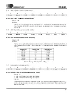
5.18.1 PLL UNLOCK (UNLOCK)

Default = 0

Function:

PLL unlock status bit. This bit will go high if the PLL becomes unlocked.

5.18.2 ADC OVERFLOW (OVERFLOW)

Default = 0

Function:

Indicates that there is an over-range condition anywhere in the CS42426 ADC signal path.

7

6

5

4

3

2

1

0

UNLOCK

Reserved

Reserved

Reserved

Reserved

Reserved

OverFlow

Reserved

Summary of Contents for CS42426

Page 1: ...internal stereo ADC is capable of independent chan nel gain control for single ended or differential analog inputs All six channels of DAC provide digital volume control and dif ferential analog outputs The general purpose outputs may be driven high or low or mapped to a variety of DAC mute controls or ADC overflow indicators The CS42426 is ideal for audio systems requiring wide dynamic range negl...

Page 2: ...us This consent does not extend to other copying such as copying for general distribution advertising or promotional purposes or for creating any work for resale An export permit needs to be obtained from the competent authorities of the Japanese Government if any of the products or technologies described in this material and controlled under the Foreign Exchange and Foreign Trade Law is to be exp...

Page 3: ...nels A2 B2 address 19h Mixing Control Pair 3 Channels A3 B3 address 1Ah 42 5 15 ADC Left Channel Gain address 1Ch 45 5 16 ADC Right Channel Gain address 1Dh 45 5 17 Interrupt Control address 1Eh 45 5 18 Interrupt Status address 20h Read Only 46 5 19 Interrupt Mask address 21h 47 5 20 Interrupt Mode MSB address 22h Interrupt Mode LSB address 23h 47 5 21 MuteC Pin Control address 28h 47 5 22 General...

Page 4: ...d Mode Transition Band 53 Figure 26 Double Speed Mode Transition Band Detail 54 Figure 27 Double Speed Mode Passband Ripple 54 Figure 28 Quad Speed Mode Stopband Rejection 54 Figure 29 Quad Speed Mode Transition Band 54 Figure 30 Quad Speed Mode Transition Band Detail 54 Figure 31 Quad Speed Mode Passband Ripple 54 Figure 32 Single Speed fast Stopband Rejection 57 Figure 33 Single Speed fast Trans...

Page 5: ...ES Table 1 PLL External Component Values 15 Table 2 Common OMCK Clock Frequencies 15 Table 3 Common PLL Output Clock Frequencies 16 Table 4 Slave Mode Clock Ratios 16 Table 5 Serial Audio Port Channel Allocations 17 Table 6 DAC De Emphasis 34 Table 7 Digital Interface Formats 35 Table 8 ADC One_Line Mode 35 Table 9 DAC One_Line Mode 35 Table 10 RMCK Divider Settings 37 Table 11 OMCK Frequency Sett...

Page 6: ... data I O line in I2 C mode and requires an external pull up resistor to the logic interface voltage as shown in the Typical Connection Diagram CDOUT is the output data line for the control port interface in SPI mode AD1 CDIN 9 Address Bit 1 I2 C Serial Control Data SPI Input AD1 is a chip address pin in I2 C mode CDIN is the input data line for the control port interface in SPI mode AD0 CS 10 Add...

Page 7: ...ring reset muting or if the master clock to left right clock frequency ratio is incorrect This pin is intended to be used as a control for external mute circuits to prevent the clicks and pops that can occur in any single supply system The use of external mute circuits are not manda tory but may be desired for designs requiring the absolute minimum in extraneous clicks and pops LPFLT 39 PLL Loop F...

Page 8: ... REFGND 19 AD0 CS 10 INT 11 Digital Audio Processor Micro Controller 56 ADC_SDOUT 48 46 44 45 47 43 AGND AGND 52 40 CFILT RFILT LPFLT 39 CRIP 2700 pF 2700 pF AINL AINL AINR AINR Left Analog Input Right Analog Input 15 16 14 13 42 See CDB42428 for a recommended filter Refer to Table 1 for proper values Connect DGND and AGND at single point near Codec GPO1 GPO2 GPO3 GPO4 GPO5 GPO6 GPO7 DAC_SDIN1 ADC...

Page 9: ...rs are required for I2 C control port operation See Note OMCK ADC_LRCK REFGND 19 AD0 CS 10 INT 11 DVD Processor 55 RMCK 58 ADCIN1 57 ADCIN2 56 ADC_SDOUT 48 46 44 45 47 43 41 4 VA VD 0 1 µF AGND AGND 52 40 CFILT RFILT LPFLT 39 CRIP 2700 pF 2700 pF AINL AINL AINR AINR Left Analog Input Right Analog Input 15 16 14 13 42 See CDB42428 for a recommended filter Refer to Table 1 for proper values Connect ...

Page 10: ...rates up to 100 kHz and uses an oversampling ratio of 64x Quad Speed mode QSM supports input sample rates up to 192 kHz and uses an oversampling ratio of 32x Using the integrated PLL a low jitter clock is recovered from the ADC LRCK input signal The recovered clock or an externally supplied clock attached to the OMCK pin can be used as the System Clock 3 2 Analog Inputs 3 2 1 Line Level Inputs AIN...

Page 11: ... will continue to be subtracted from the conversion result This feature makes it possible to perform a system DC offset calibration by 1 Running the CS42426 with the high pass filter enabled until the filter settles See the Digital Filter Characteristics for filter settling time 2 Disabling the high pass filter and freezing the stored DC offset The high pass filters are controlled using the HPF_FR...

Page 12: ...n increments of 0 125 dB at the rate controlled by the SZC 1 0 bits in the Digital Volume Control register See Volume Control address 0Dh on page 40 Each output can be independently muted via mute control bits in the register Channel Mute address 0Eh on page 41 When enabled each XX_MUTE bit attenuates the corresponding DAC to its maximum value 127 dB When the XX_MUTE bit is disabled the correspond...

Page 13: ...ontrol addresses 29h to 2Fh on page 48 3 3 4 ATAPI Specification The CS42426 implements the channel mixing functions of the ATAPI CD ROM specification The ATAPI functions are applied per A B pair Refer to Table 15 on page 44 and Figure 5 for additional infor mation Σ Σ A Channel Volume Control AOUTAx AOUTBx Left Channel Audio Data Right Channel Audio Data B Channel Volume Control MUTE MUTE DAC_SDI...

Page 14: ...K bit to a 1 in the register Clock Control address 06h on page 37 the PLL will lock to the incoming ADC_LRCK and generate an output master clock RMCK of 256Fs Table 3 below shows the output of the PLL with typical input Fs values for ADC_LRCK The PLL behavior is affected by the external filter component values Figure 1 shows the required config uration of the external filter components The set of ...

Page 15: ...CK or the output of the PLL with an input reference to the ADC_LRCK input from the ADC serial port The DAC Serial Port and ADC Serial Port can both be masters only when OMCK is used as the clock source When using the PLL output the ADC Serial Port must be slave and the DAC Serial Port can operate in Master Mode Master clock selection and operation is configured with the SW_CTRL1 0 and CLK_SEL bits...

Page 16: ...udio data Either ADC_SCLK or DAC_SCLK can be generated by the CS42426 master mode or it can be input from an external source slave mode Master or Slave mode selection is made using bits DAC_SP M S and ADC_SP M S in register Misc Control address 05h on page 36 The Left Right clock ADC_LRCK or DAC_LRCK is used to indicate left and right data frames and the start of a new sample period It may be an o...

Page 17: ...Cs When operated in One Line Data Mode 6 channels of DAC data are input on DAC_SDIN1 and 6 channels of ADC data are output on ADC_SDOUT Table 5 outlines the serial port channel allocations Serial Inputs Outputs DAC_SDIN1 left channel right channel one line mode DAC 1 DAC 2 DAC channels 1 2 3 4 5 6 DAC_SDIN2 left channel right channel one line mode DAC 3 DAC 4 not used DAC_SDIN3 left channel right ...

Page 18: ...quivalent to Fs 32 44 1 48kHz double speed mode is for Fs 64 88 2 96 kHz and quad speed mode is for Fs 176 4 196 kHz Left Channel Right Channel 6 5 4 3 2 1 0 9 8 7 15 14 13 12 11 10 6 5 4 3 2 1 0 9 8 7 15 14 13 12 11 10 DAC_SDINx ADC_SDOUT DAC_LRCK ADC_LRCK DAC_SCLK ADC_SCLK Figure 7 Right Justified Serial Audio Formats Right Justified Mode Data Valid on Rising Edge of SCLK Bits Sample SCLK Rate s...

Page 19: ...s 48 64 128 Fs single speed mode 64 Fs 64 Fs double speed mode 64 Fs 64 Fs quad speed mode DAC_LRCK ADC_LRCK DAC_SCLK ADC_SCLK Left Channel Right Channel DAC_SDINx ADC_SDOUT 3 2 1 5 4 1 2 3 4 5 3 2 1 5 4 1 2 3 4 MSB LSB MSB LSB Figure 9 Left Justified Serial Audio Formats Left Justified Mode Data Valid on Rising Edge of SCLK Bits Sample SCLK Rate s Notes Master Slave 16 64 Fs 32 48 64 128 Fs singl...

Page 20: ... of SCLK Bits Sample SCLK Rate s Notes Master Slave 20 128 Fs 128 Fs single speed mode 128 Fs 128Fs double speed mode DAC_LRCK ADC_LRCK DAC_SCLK ADC_SCLK LSB MSB 24 clks 128 clks LSB MSB LSB MSB LSB MSB LSB MSB LSB MSB MSB DAC1 DAC3 DAC5 DAC2 DAC4 DAC6 24 clks 24 clks 24 clks 24 clks 24 clks Left Channel Right Channel 24 clks ADC1 ADC3 ADC5 ADC2 ADC4 ADC6 24 clks 24 clks 24 clks 24 clks 24 clks AD...

Page 21: ...ion the CS42426 must be configured to select which SCLK LRCK is being used to clock the external ADCs The EXT ADC SCLK bit in register Misc Control address 05h on page 36 must be set accordingly Set this bit to 1 if the external ADCs are wired using the DAC_SP clocks If the ADCs are wired to use the ADC_SP clocks set this bit to 0 DAC_LRCK ADC_LRCK DAC_SCLK ADC_SCLK Left Channel Right Channel ADCI...

Page 22: ... combinations Misc Control Register addr 05h Set DAC_SP M S 1 Configure DAC Serial Port to master mode Set ADC_SP M S 1 Configure ADC Serial Port to master mode Set EXT ADC SCLK 0 Identify external ADC clock source as ADC Serial Port DAC Mode Not One Line Mode One Line Mode 1 One Line Mode 2 ADC Mode Not One Line Mode DAC_SCLK 64Fs DAC_LRCK SSM DSM QSM DAC_SCLK 128Fs DAC_LRCK SSM DSM ADC_SCLK 64Fs...

Page 23: ..._OLx bits 00 01 Select DAC operating mode see table below for valid combinations Misc Control Register addr 05h Set CODEC_SP M S 1 Set CODEC Serial Port to master mode Set SAI_SP M S 1 Set Serial Audio Interface Port to master mode Set EXT ADC SCLK 1 Identify external ADC clock source as DAC Serial Port DAC Mode Not One Line Mode One Line Mode 1 One Line Mode 2 ADC Mode Not One Line Mode DAC_SCLK ...

Page 24: ...combinations Set DAC_OLx bits 00 01 10 Select DAC operating mode see table below for valid combinations Misc Control Register addr 05h Set DAC_SP M S 1 Set DAC Serial Port to master mode Set ADC_SP M S 0 or 1 Set ADC Serial Port to master mode or slave mode Set EXT ADC SCLK 0 Identify external ADC clock source as ADC Serial Port DAC Mode Not One Line Mode One Line Mode 1 One Line Mode 2 ADC Mode N...

Page 25: ...Set ADC operating mode to Not One Line Mode since only 2 channels of ADC are supported Set DAC_OLx bits 00 01 10 Select DAC operating mode see table below for valid combinations Misc Control Register addr 05h Set DAC_SP M S 0 or 1 Set DAC Serial Port to master mode or slave mode Set ADC_SP M S 0 or 1 Set ADC Serial Port to master mode or slave mode Set EXT ADC SCLK 0 External ADCs are not used Lea...

Page 26: ...operation of the control port in SPI mode To write to a register bring CS low The first seven bits on CDIN form the chip address and must be 1001111 The eighth bit is a read write indi cator R W which should be low to write The next eight bits form the Memory Address Pointer MAP which is set to the address of the register that is to be updated The next eight bits are the data which will be placed ...

Page 27: ... the 7 bit address field are fixed at 10011 To communicate with a CS42426 the chip address field which is the first byte sent to the CS42426 should match 10011 followed by the settings of the AD1 and AD0 The eighth bit of the address is the R W bit If the operation is a write the next byte is the Memory Address Pointer MAP which selects the register to be read or written If the op eration is a rea...

Page 28: ...es of consecutive registers Each byte is separated by an acknowledge bit 3 7 Interrupts The CS42426 has a comprehensive interrupt capability The INT output pin is intended to drive the inter rupt input pin on the host microcontroller The INT pin may be set to be active low active high or active low with no active pull up transistor This last mode is used for active low wired OR hook ups with mul t...

Page 29: ...ay all serial ports and DAC outputs will be automatically muted 3 9 Power Supply Grounding and PCB layout As with any high resolution converter the CS42426 requires careful attention to power supply and ground ing arrangements if its potential performance is to be realized Figure 1 shows the recommended power arrangements with VA connected to clean supplies VD which powers the digital circuitry ma...

Page 30: ... Control Reserved SNGVOL SZC1 SZC0 AMUTE Reserved RAMP_UP RAMP_DN default 0 0 0 0 1 0 0 0 0Eh Channel Mute Reserved Reserved B3_MUTE A3_MUTE B2_MUTE A2_MUTE B1_MUTE A1_MUTE default 0 0 0 0 0 0 0 0 0Fh Vol Control A1 A1_VOL7 A1_VOL6 A1_VOL5 A1_VOL4 A1_VOL3 A1_VOL2 A1_VOL1 A1_VOL0 default 0 0 0 0 0 0 0 0 10h Vol Control B1 B1_VOL7 B1_VOL6 B1_VOL5 B1_VOL4 B1_VOL3 B1_VOL2 B1_VOL1 B1_VOL0 default 0 0 0...

Page 31: ... 22h Interrupt Mode MSB UNLOCK1 Reserved Reserved Reserved Reserved Reserved OF1 Reserved default 0 0 0 0 0 0 0 0 23h Interrupt Mode LSB UNLOCK0 Reserved Reserved Reserved Reserved Reserved OF0 Reserved default 0 0 0 0 0 0 0 0 24h 27h Reserved Reserved Reserved Reserved Reserved Reserved Reserved Reserved Reserved default 0 0 0 0 0 0 0 0 28h MUTEC Reserved Reserved MCPolarity M_AOUTA1 M_AOUTB1 M_A...

Page 32: ...ncrement control 0 MAP is not incremented automatically 1 Internal MAP is automatically incremented after each read or write 5 1 2 MEMORY ADDRESS POINTER MAPX Default 0000001 Function Memory address pointer MAP Sets the register address that will be read or written by the control port 5 2 Chip I D and Revision Register address 01h Read Only 5 2 1 CHIP I D CHIP_IDX Default 1110 Function I D code fo...

Page 33: ...remain in a reset state 5 3 4 POWER DOWN PDN Default 1 Function The entire device will enter a low power state when this function is enabled and the contents of the control registers are retained in this mode The power down bit defaults to enabled on power up and must be disabled before normal operation can occur 5 4 Functional Mode address 03h 5 4 1 DAC FUNCTIONAL MODE DAC_FMX Default 00 00 Singl...

Page 34: ... 32 44 1 or 48 kHz De emphasis will not be enabled regard less of this register setting at any other sample rate If the FRC_PLL_LK bit is set to a 1 b then the auto detect sample rate feature is disabled To apply the correct de emphasis filter use the DE EMPH bits in the Interrupt Control address 1Eh register to set the appropriate sample rate 5 5 Interface Formats address 04h 5 5 1 DIGITAL INTERF...

Page 35: ...ITS CODEC_RJ16 Default 0 Function This bit determines how many bits to use during right justified mode for the DAC and ADC By default the DAC and ADC will be in RJ24 bits but can be set to RJ16 bits 0 24 bit mode 1 16 bit mode DIF1 DIF0 Description Format Figure 0 0 Left Justified up to 24 bit data 0 9 0 1 I2 S up to 24 bit data 1 8 1 0 Right Justified 16 bit or 24 bit data 2 7 1 1 reserved Table ...

Page 36: ...rs without the changes taking effect until the FREEZE is disabled To make multiple changes in these control port registers take effect simultaneously enable the FREEZE bit make all register changes then disable the FREEZE bit 5 6 4 INTERPOLATION FILTER SELECT FILT_SEL Default 0 Function This feature allows the user to select whether the DAC interpolation filter has a fast or slow roll off For filt...

Page 37: ...nd ADC_LRCK become inputs To use the PLL to lock to ADC_LRCK the ADC_SP must be in slave mode When using the PLL to lock to LRCK if ADC_SDOUT is configured to be clocked by the ADC_SP then both ADC_SCLK and ADC_LRCK must be present If ADC_SDOUT is configured to be clocked by the DAC_SP then only the ADC_LRCK signal must be applied 5 7 Clock Control address 06h 5 7 1 RMCK DIVIDE RMCK_DIVX Default 0...

Page 38: ...port timings are not valid 5 7 5 FORCE PLL LOCK FRC_PLL_LK Default 0 Function This bit is used to enable the PLL to lock to the ADC_LRCK with the absence of a clock signal on OMCK When set to a 1 b the auto detect sample frequency feature will be disabled The OM CK PLL_CLK Ratio address 07h Read Only register contents are not valid and the PLL_CLK 2 0 bits will be set to 111 b Use the DE EMPH 1 0 ...

Page 39: ...etween the OMCK and the recovered clock from the PLL which is displayed in register 07h Based on this ratio the absolute frequency of the PLL clock can be determined and this information is displayed according to the following table If the absolute fre quency of the PLL clock does not match one of the given frequencies this register will display the closest available value NOTE These bits are set ...

Page 40: ...a timeout period between 512 and 1024 sample periods 10 7 ms to 21 3 ms at 48 kHz sample rate if the signal does not encounter a zero crossing The zero cross function is independently mon itored and implemented for each channel Soft Ramp Soft Ramp allows level changes both muting and attenuation to be implemented by incrementally ramping in 1 8 dB steps from the current level to the new level at a...

Page 41: ...te un mute is performed in these instances Note For best results it is recommended that this bit be used in conjunction with the RMP_DN bit 5 10 5 SOFT RAMP DOWN BEFORE FILTER MODE CHANGE RMP_DN Default 0 0 Disabled 1 Enabled Function A mute will be performed prior to executing a filter mode or de emphasis mode change When this feature is enabled this mute is affected similar to attenuation change...

Page 42: ...SIGNAL POLARITY INV_XX Default 0 0 Disabled 1 Enabled Function When enabled these bits will invert the signal polarity of their respective channels 5 14 Mixing Control Pair 1 Channels A1 B1 address 18h Mixing Control Pair 2 Channels A2 B2 address 19h Mixing Control Pair 3 Channels A3 B3 address 1Ah 7 6 5 4 3 2 1 0 xx_VOL7 xx_VOL6 xx_VOL5 xx_VOL4 xx_VOL3 xx_VOL2 xx_VOL1 xx_VOL0 Binary Code Decimal ...

Page 43: ...Bx volume levels are independently controlled by the A and the B Channel Volume Control registers when this function is disabled The volume on both AOUTAx and AOUTBx are determined by the A Channel Volume Control registers per A B pair and the B Channel Volume Control registers are ignored when this function is enabled ...

Page 44: ... 1 1 MUTE b L R 2 0 0 1 0 0 aR MUTE 0 0 1 0 1 aR bR 0 0 1 1 0 aR bL 0 0 1 1 1 aR b L R 2 0 1 0 0 0 aL MUTE 0 1 0 0 1 aL bR 0 1 0 1 0 aL bL 0 1 0 1 1 aL b L R 2 0 1 1 0 0 a L R 2 MUTE 0 1 1 0 1 a L R 2 bR 0 1 1 1 0 a L R 2 bL 0 1 1 1 1 a L R 2 b L R 2 1 0 0 0 0 MUTE MUTE 1 0 0 0 1 MUTE bR 1 0 0 1 0 MUTE bL 1 0 0 1 1 MUTE aL bR 2 1 0 1 0 0 aR MUTE 1 0 1 0 1 aR bR 1 0 1 1 0 aR bL 1 0 1 1 1 aR bL aR 2...

Page 45: ... 17 Interrupt Control address 1Eh 5 17 1 SERIAL PORT SYNCHRONIZATION SP_SYNC Default 0 0 DAC ADC Serial Port timings not in phase 1 DAC ADC Serial Port timings are in phase Function Forces the LRCK and SCLK from the DAC ADC Serial Ports to align and operate in phase This function will operate when both ports are running at the same sample rate or when operating at dif ferent sample rates 7 6 5 4 3...

Page 46: ...nterrupt pin INT will indicate an interrupt condition 5 18 Interrupt Status address 20h Read Only For all bits in this register a 1 means the associated interrupt condition has occurred at least once since the register was last read A 0 means the associated interrupt condition has NOT occurred since the last reading of the register Reading the register resets all bits to 0 Status bits that are mas...

Page 47: ...on In the Rising edge active mode the INT pin becomes active on the arrival of the interrupt condition In the Falling edge active mode the INT pin becomes active on the removal of the interrupt condition In Level active mode the INT interrupt pin becomes active during the interrupt condition Be aware that the active level Active High or Low only depends on the INT 1 0 bits located in the register ...

Page 48: ...put driven low or as a dedicated ADC overflow pin indicating an over range condition anywhere in the ADC signal path for either the left or right channel The Functionx bits determine the operation of the pin When configured as a GPO with the output driven low the driver is a CMOS driver When configured to identify an ADC Overflow condition the driver is an open drain driver requiring a pull up res...

Page 49: ...ut then the functional bits are ignored and the pin is driven high It is recommended that in this mode all the functional bits be set to 0 GPOx Reg Address Function4 Function3 Function2 Function1 Function0 GPO7 pin 42 29h M_AOUTA1 M_AOUTB1 M_AOUTA2 M_AOUTB2 M_AOUTA3 M_AOUTB3 Reserved GPO6 pin 43 2Ah M_AOUTA1 M_AOUTB1 M_AOUTA2 M_AOUTB2 M_AOUTA3 M_AOUTB3 Reserved GPO5 pin 44 2Bh M_AOUTA1 M_AOUTB1 M_...

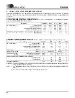
Page 50: ...ause SCR latch up 2 The maximum over under voltage is limited by the input current Parameter Symbol Min Typ Max Units DC Power Supply Analog power Digital internal power Serial data port interface power Control port interface power VA VD VLS VLC 4 75 3 13 1 8 1 8 5 0 3 3 5 0 5 0 5 25 5 25 5 25 5 25 V V V V Ambient Operating Temperature power applied CS42426 CQ CS42426 DQ TA 10 40 70 85 C C Paramet...

Page 51: ...08 dB dB dB Total Harmonic Distortion Noise Note 4 1 dB 20 dB 60 dB 40kHz bandwidth 1 dB THD N 100 91 51 97 94 100 91 51 97 92 dB dB dB dB Quad Speed Mode Fs 192 kHz Dynamic Range A weighted unweighted 40 kHz bandwidth unweighted 108 105 114 111 108 106 103 114 111 108 dB dB dB Total Harmonic Distortion Noise Note 4 1 dB 20 dB 60 dB 40 kHz bandwidth 1 dB THD N 100 91 51 97 94 100 91 51 97 92 dB dB...

Page 52: ... 0 035 dB Stopband Note 6 0 58 Fs Stopband Attenuation 95 dB Total Group Delay Fs Output Sample Rate tgd 12 Fs s Group Delay Variation vs Frequency tgd 0 0 µs Double Speed Mode 50 to 100 kHz sample rates Passband 0 1 dB Note 6 0 0 45 Fs Passband Ripple 0 035 dB Stopband Note 6 0 68 Fs Stopband Attenuation 92 dB Total Group Delay Fs Output Sample Rate tgd 9 Fs s Group Delay Variation vs Frequency t...

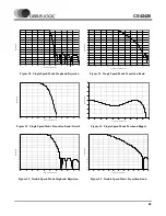
Page 53: ...55 Frequency normalized to Fs Amplitude dB 0 10 0 08 0 05 0 03 0 00 0 03 0 05 0 08 0 10 0 00 0 05 0 10 0 15 0 20 0 25 0 30 0 35 0 40 0 45 0 50 Frequency normalized to Fs Amplitude dB Figure 22 Single Speed Mode Transition Band Detail Figure 23 Single Speed Mode Passband Ripple 140 130 120 110 100 90 80 70 60 50 40 30 20 10 0 0 0 0 1 0 2 0 3 0 4 0 5 0 6 0 7 0 8 0 9 1 0 Frequency normalized to Fs Am...

Page 54: ... 0 7 0 8 0 9 1 0 Frequency normalized to Fs Amplitude dB 130 120 110 100 90 80 70 60 50 40 30 20 10 0 0 2 0 25 0 3 0 35 0 4 0 45 0 5 0 55 0 6 0 65 0 7 0 75 0 8 Frequency normalized to Fs Amplitude dB Figure 28 Quad Speed Mode Stopband Rejection Figure 29 Quad Speed Mode Transition Band 10 9 8 7 6 5 4 3 2 1 0 0 1 0 15 0 2 0 25 0 3 0 35 0 4 0 45 0 5 0 55 0 6 Frequency normalized to Fs Amplitude dB 0...

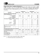
Page 55: ...x CS42426 DQ Min Typ Max Unit Dynamic performance for all modes Dynamic Range Note 8 24 bit A weighted unweighted 16 bit A Weighted Note 9 unweighted 108 105 114 111 97 94 108 105 114 111 97 94 dB dB dB dB Total Harmonic Distortion Noise 24 bit 0 dB 20 dB 60 dB 16 bit 0 dB Note 9 20 dB 60 dB THD N 100 91 51 94 74 34 94 100 91 51 94 74 34 94 dB dB dB dB dB dB Idle Channel Noise Signal to noise rati...

Page 56: ...uation Note 11 90 64 dB Group Delay 12 Fs 6 5 Fs s Passband Group Delay Deviation 0 20 kHz 0 41 Fs 0 14 Fs s De emphasis Error Note 12 Fs 32 kHz Relative to 1 kHz Fs 44 1 kHz Fs 48 kHz 0 23 0 14 0 09 0 23 0 14 0 09 dB dB dB Combined Digital and On chip Analog Filter Response Double Speed Mode 96 kHz Passband Note 10 to 0 01 dB corner to 3 dB corner 0 0 0 4166 0 4998 0 0 0 2083 0 4998 Fs Fs Frequen...

Page 57: ... 4 3 2 1 0 Frequency normalized to Fs Amplitude dB 0 0 05 0 1 0 15 0 2 0 25 0 3 0 35 0 4 0 45 0 5 0 02 0 015 0 01 0 005 0 0 005 0 01 0 015 0 02 Frequency normalized to Fs Amplitude dB Figure 34 Single Speed fast Transition Band detail Figure 35 Single Speed fast Passband Ripple 0 4 0 5 0 6 0 7 0 8 0 9 1 120 100 80 60 40 20 0 Frequency normalized to Fs Amplitude dB 0 4 0 42 0 44 0 46 0 48 0 5 0 52 ...

Page 58: ...40 20 0 Frequency normalized to Fs Amplitude dB 0 4 0 42 0 44 0 46 0 48 0 5 0 52 0 54 0 56 0 58 0 6 120 100 80 60 40 20 0 Frequency normalized to Fs Amplitude dB Figure 40 Double Speed fast Stopband Rejection Figure 41 Double Speed fast Transition Band 0 45 0 46 0 47 0 48 0 49 0 5 0 51 0 52 0 53 0 54 0 55 10 9 8 7 6 5 4 3 2 1 0 Frequency normalized to Fs Amplitude dB 0 0 05 0 1 0 15 0 2 0 25 0 3 0...

Page 59: ...9 8 7 6 5 4 3 2 1 0 Frequency normalized to Fs Amplitude dB 0 0 05 0 1 0 15 0 2 0 25 0 3 0 35 0 02 0 015 0 01 0 005 0 0 005 0 01 0 015 0 02 Frequency normalized to Fs Amplitude dB Figure 46 Double Speed slow Transition Band detail Figure 47 Double Speed slow Passband Ripple 0 2 0 3 0 4 0 5 0 6 0 7 0 8 0 9 1 120 100 80 60 40 20 0 Frequency normalized to Fs Amplitude dB 0 2 0 3 0 4 0 5 0 6 0 7 0 8 1...

Page 60: ...00 80 60 40 20 0 Frequency normalized to Fs Amplitude dB 0 1 0 2 0 3 0 4 0 5 0 6 0 7 0 8 0 9 120 100 80 60 40 20 0 Frequency normalized to Fs Amplitude dB Figure 52 Quad Speed slow Stopband Rejection Figure 53 Quad Speed slow Transition Band 0 45 0 46 0 47 0 48 0 49 0 5 0 51 0 52 0 53 0 54 0 55 10 9 8 7 6 5 4 3 2 1 0 Frequency normalized to Fs Amplitude dB 0 0 02 0 04 0 06 0 08 0 1 0 12 0 02 0 015...

Page 61: ... Duty Cycle 45 50 55 Master Mode RMCK to DAC_SCLK ADC_SCLK active edge delay tsmd 0 10 ns RMCK to DAC_LRCK ADC_LRCK delay tlmd 0 10 ns Slave Mode DAC_SCLK ADC_SCLK Falling Edge to ADC_SDOUT ADC_SDOUT Output Valid tdpd 50 ns DAC_LRCK ADC_LRCK Edge to MSB Valid tlrpd 20 ns DAC_SDIN Setup Time Before DAC_SCLK Rising Edge tds 10 ns DAC_SDIN Hold Time After DAC_SCLK Rising Edge tdh 30 ns DAC_SCLK ADC_S...

Page 62: ...o Start tirs 500 ns Bus Free Time Between Transmissions tbuf 4 7 µs Start Condition Hold Time prior to first clock pulse thdst 4 0 µs Clock Low time tlow 4 7 µs Clock High Time thigh 4 0 µs Setup Time for Repeated Start Condition tsust 4 7 µs SDA Hold Time from SCL Falling Note 16 thdd 0 µs SDA Setup time to SCL Rising tsud 250 ns Rise Time of SCL and SDA trc 1 µs Fall Time SCL and SDA tfc 300 ns ...

Page 63: ...al to 1 024 MHz should be safe for all possible conditions 20 Data must be held for sufficient time to bridge the transition time of CCLK 21 For fsck 1 MHz Parameter Symbol Min Typ Max Units CCLK Clock Frequency Note 19 fsck 0 6 0 MHz CS High Time Between Transmissions tcsh 1 0 µs CS Falling to CCLK Edge tcss 20 ns CCLK Low Time tscl 66 ns CCLK High Time tsch 66 ns CDIN to CCLK Rising Setup Time t...

Page 64: ...z limit the loading on the signal to 1 CMOS load Parameter Symbol Min Typ Max Units Power Supply Current normal operation VA 5 V Note 22 VD 5 V VD 3 3 V Interface current VLC 5V Note 23 VLS 5 V power down state all supplies Note 24 IA ID ID ILC ILS Ipd 90 150 100 250 250 250 mA mA mA µA µA µA Power Consumption Note 22 VA 5 V VD VLS VLC 3 3 V normal operation power down Note 24 VA 5 V VD VLS VLC 5 ...

Page 65: ...spectral components over the specified band width typically 10 Hz to 20 kHz including distortion components Expressed in decibels Measured at 1 and 20 dBFS as suggested in AES17 1991 Annex A Frequency Response A measure of the amplitude response variation from 10 Hz to 20 kHz relative to the amplitude response at 1 kHz Units in decibels Interchannel Isolation A measure of crosstalk between the lef...

Page 66: ...rrus Logic The Effects of Sampling Clock Jitter on Nyquist Sampling Analog to Digital Convert ers and on Oversampling Delta Sigma ADC s by Steven Harris Paper presented at the 87th Conven tion of the Audio Engineering Society October 1989 6 Cirrus Logic An 18 Bit Dual Channel Oversampling Delta Sigma A D Converter with 19 Bit Mono Application Example by Clif Sanchez Paper presented at the 87th Con...

Page 67: ... 9 90 10 0 BSC 10 10 E 0 461 0 472 BSC 0 484 11 70 12 0 BSC 12 30 E1 0 390 0 393 BSC 0 398 9 90 10 0 BSC 10 10 e 0 016 0 020 BSC 0 024 0 40 0 50 BSC 0 60 L 0 018 0 024 0 030 0 45 0 60 0 75 0 000 4 7 000 0 00 4 7 00 Nominal pin pitch is 0 50 mm Controlling dimension is mm JEDEC Designation MS022 Parameter Symbol Min Typ Max Units Allowable Junction Temperature 135 C Junction to Ambient Thermal Impe...

Reviews: