8
DS632F1
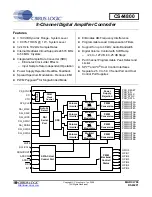
CS44800
1. CHARACTERISTICS AND SPECIFICATIONS
(All Min/Max characteristics and specifications are guaranteed over the Specified Operating Conditions. Typical
performance characteristics and specifications are derived from measurements taken at nominal supply voltages
and T
A
= 25
°
C.)
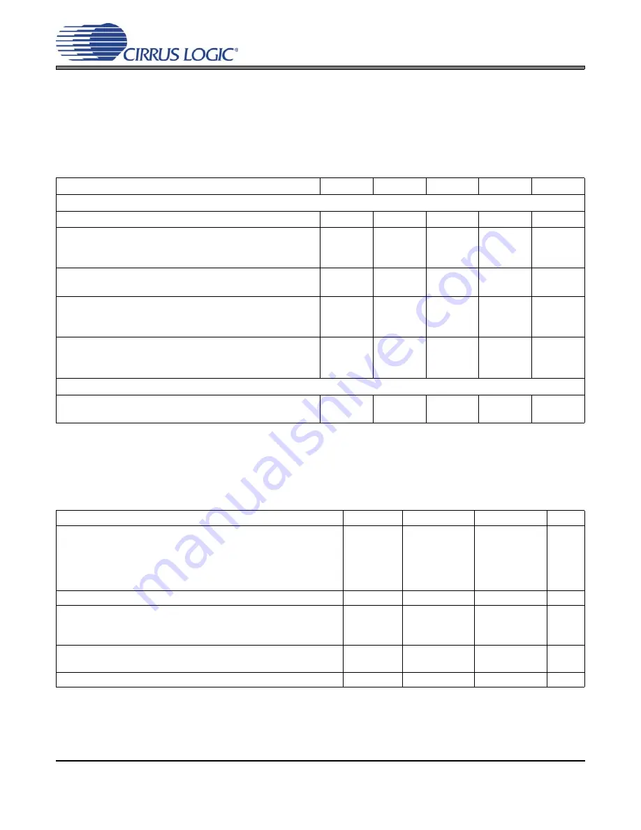
SPECIFIED OPERATING CONDITIONS
(GND = 0 V, all voltages with respect to ground)
Notes:
1.
When using external crystal, VDX = 3.14 V(min). When using clock signal input, VDX = 2.37 V(min).
ABSOLUTE MAXIMUM RATINGS
(GND = 0 V; all voltages with respect to ground.)
WARNING:
Operation at or beyond these limits may result in permanent damage to the device. Normal operation
is not guaranteed at these extremes.
2.
Any pin except supplies. Transient currents of up to ±100 mA on the input pins will not cause SCR latch-up.
3.
The maximum over/under voltage is limited by the input current.
Parameter
Symbol
Min
Typ
Max
Units
DC Power Supply
Digital
2.5 V
VD
2.37
2.5
2.63
V
XTAL
2.5 V
3.3 V
5.0 V
VDX
2.37
3.14
4.75
2.5
3.3
5.0
2.63
3.47
5.25
V
V
V
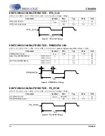
PWM Interface
3.3 V
5.0 V
VDP
3.14
4.75
3.3
5.0
3.47
5.25
V
V
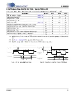
Serial Audio Interface
2.5 V
3.3 V
5.0 V
VLS
2.37
3.14
4.75
2.5
3.3
5.0
2.63
3.47
5.25
V
V
V
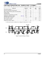
Control Interface
2.5 V
3.3 V
5.0 V
VLC
2.37
3.14
4.75
2.5
3.3
5.0
2.63
3.47
5.25
V
V
V
Ambient Operating Temperature
Commercial
-CQZ
Automotive
-DQZ
T
A
-10
-40
-
-
+70
+85
°
C
°
C
Parameters
Symbol
Min
Max
Units
DC Power Supply
Digital
XTAL
PWM Interface
Serial Audio Interface
Control Interface
VD
VDX
VDP
VLS
VLC
-0.3
-0.3
-0.3
-0.3
-0.3
3.5
6.0
6.0
6.0
6.0
V
V
V
V
V
Input Current
I
in
-
±10
mA
Digital Input Voltage
PWM Interface
Serial Audio Interface
Control Interface
V
IND-PWM
V
IND-S
V
IND-C
-0.3
-0.3
-0.3
VDP+0.4
VLS+0.4
VLC+0.4
V
V
V
Ambient Operating Temperature
-CQ
(power applied)
-DQ
T
A
-20
-50
+85
+95
°C
°C
Storage Temperature
T
stg
-65
+150
°C