DS726PP2
63
CS4525
6.6.3
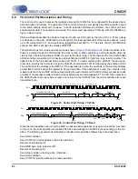
Right-Justified Data Format
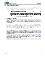
In Right-Justified format, data is received most significant bit first and with the least significant bit present-
ed on the last SCLK before the LRCK transition and is valid on the rising edge of SCLK. For the Right-
Justified format, the left channel data is presented when LRCK is high and the right channel data is pre-
sented when LRCK is low. 16, 18, 20, and 24 bits per sample are supported.
6.7
Integrated VD Regulator
The CS4525 includes two internal linear regulators, one from the VD supply voltage to provide a fixed
supply to its internal digital blocks, and another from the VD supply voltage to provide a fixed
supply
to its internal analog blocks. The LVD pin must be set to indicate the voltage present on the VD pin as shown
in
The output of the digital regulator is presented on the VD_REG pin and may be used to provide an external
device with up to
of current at its nominal output voltage of
. The output of the analog regulator
is presented on the VA_REG pin and must only be connected to the bypass capacitors as shown in the typ-
ical connection diagrams.
If a nominal supply voltage of 2.5 V is used as the VD supply (see the
Recommended Operating Conditions
table on
), the VD, VD_REG, and VA_REG pins must all be connected to the VD supply source. In
this configuration, the internal regulators are bypassed and the external supply source is used to directly
drive the internal digital and analog sections.
VD
Connection
VD_REG
Connection
VA_REG
Connection
LVD
Connection
SelectVD Bit Setting
Software Mode Only
5 V Supply
Bypass Capacitors Only
Bypass Capacitors Only
VD
‘1’ - Default
3.3 V Supply
Bypass Capacitors Only
Bypass Capacitors Only
DGND
‘1’ - Default
2.5 V Supply
VD and Bypass Capacitors
VD and Bypass Capacitors
DGND
‘0’
Table 21. Power Supply Configuration and Settings
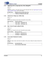
Referenced Control
Register Location
SelectVD .............................
“Select VD Level (SelectVD)” on page 88
Left Channel
Right Channel
6
5
4
3
2
1
0
9
8
7
15 14 13 12 11 10
6
5
4
3
2
1
0
9
8
7
15 14 13 12 11 10
SDIN
LRCK
SCLK
Figure 32. Right-Justified Serial Audio Formats

