18
DS726PP2
CS4525
5. CHARACTERISTICS AND SPECIFICATIONS
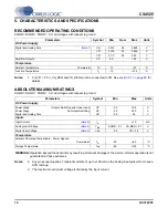
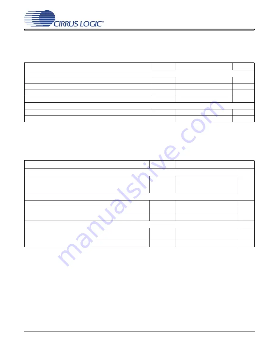
RECOMMENDED OPERATING CONDITIONS
AGND = DGND = PGND = 0 V; all voltages with respect to ground.
Notes:
1.
For VD = 2.5 V, VA_REG and VD_REG must be connected to VD. See
for
details.
ABSOLUTE MAXIMUM RATINGS
AGND = DGND = PGND = 0 V; all voltages with respect to ground.
WARNING:
Operation beyond these limits may result in permanent damage to the device. Normal operation is not
guaranteed at these extremes.
Notes:
2.
Any pin except supplies. Transient currents of up to ±100 mA on the analog input pins will not cause
SCR latch-up.
3.
The maximum over/under voltage is limited by the input current.
Parameters
Symbol Min Nom
Max
Units
DC Power Supply
Digital and Analog Core
VD
2.375
2.5
2.625
V
VD
3.135
3.3
3.465
V
VD
4.75
5.0
5.25
V
Amplifier Outputs
VP
8.0
-
18.0
V
Temperature
Ambient Temperature
Commercial
T
A
-10
-
+70
°
C
Junction Temperature
T
J
-10
-
+125
°
C
Parameters
Symbol
Min
Max
Units
DC Power Supply
Power Stage
Outputs Switching and Under Load
Power Stage
No Output Switching
Digital and Analog Core
VP
VP
VD
-0.3
-0.3
-0.3
19.8
23.0
6.0
V
V
V
Inputs
Input Current
I
in
-
±10
mA
Analog Input Voltage
V
INA
AGND - 0.7
0.7
V
Digital Input Voltage
V
IND
-0.3
VD + 0.4
V
Temperature
Ambient Operating Temperature - Power Applied
Commercial
T
A
-20
+85
°C
Storage Temperature
T
stg
-65
+150
°C


