9-1
Copyright 2009 Cirrus Logic, Inc.
DS734UM7
Typical Connection Diagrams
CS485xx Hardware User’s Manual
Chapter 8
System Integration
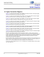
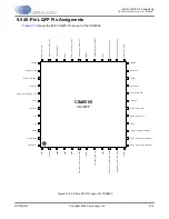
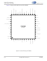
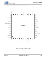
9.1 Typical Connection Diagrams
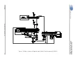
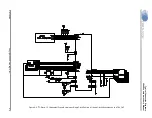
Figure 9-1
is a typical connection diagram for the CS485xx in SPI slave mode with 10 channels of digital
audio input and all audio clocks synchronous to S/PDIF RX.
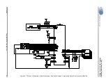
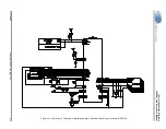
Figure 9-2
is a typical connection diagram for the CS485xx in I
2
C slave mode with 10 channels of digital
audio input, dual-clock domain, output audio clocks synchronous to HDMI Rx.
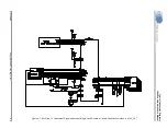
Figure 9-3
is a typical connection diagram for the CS485xx in I
2
C slave mode with 12 channels of digital
audio input, a single-clock domain, and all audio clocks synchronous to XTAL_OUT.
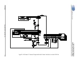
Figure 9-4
is a typical connection diagram for the CS485xx in I
2
C master mode with 10 channels of digital
audio input and all audio clocks synchronous to S/PDIF Rx.
Figure 9-5
is a typical connection diagram for the CS485xx in SPI slave mode with 10 channels of digital
audio input and all Audio Clocks Synchronous to S/PDIF Rx.
Figure 9-6
is a typical connection diagram for the CS485xx in SPI slave mode with 10 channels of digital
audio input, dual clock domains, and output audio clocks synchronous to HDMI Rx.
Figure 9-7
is a typical connection diagram for the CS485xx in SPI slave mode with 12 channels of digital
audio input, a single clock domain, and all audio clocks synchronous to XTAL_OUT.
Figure 9-8
is a typical connection diagram for the CS485xx in SPI master mode with 10 channels of digital
audio input and all audio clocks synchronous to S/PDIF Rx.
Place PLL current reference resistor as close as possible to the DSP. A unified, solid ground plane is
recommended for optimal performance. Pay close attention to the direction of all clock signals shown in the
diagram. These designs are configured to slave to clocks on the input side. On the output side, the DSP
slaves to MCLK from the S/PDIF receiver and masters SCLK and LRCLK for the DACs. This is the
recommended clocking for AVR applications.
Series Termination resistor values depend on the transmission line impedances of the actual PCB used. The
design engineer should calculate the transmission line impedance of the traces and size the series R such
that R = (Z – 20), where 20 represents the source impedance of the CS485xx drivers.
The typical connection diagrams show “0.1uF x 3” to indicate that 1 decoupling capacitor should be placed
next to each power pin.


