CDB4923 CDB49300
10
DS262DB2
The two major PLD modes for the CDB4923/300
are the PROVIDED resource mode and the EX-
TERNAL interface mode. When a PROVIDED
mode is chosen all clocks are provided by the dem-
onstration board, all audio data passes through the
PLD, and the DSP is controlled by the PC parallel
port interface. The EXTERNAL interface modes
allow the user to drive the audio data and control
pins of the DSP directly by wire-wrapping to stake
headers J11 and J12, bypassing the control PLD. It
should be noted that there are two variants of the
EXTERNAL interface mode. One EXTERNAL
mode provides direct access to all control and audio
data input pins of the CS492x/CS493xx, and the
second EXTERNAL mode allows the user to drive
the control signals of the CS492x/CS493xx while
audio data still comes from the CDB4923/300.
The DIP switch S3 is used to choose the different
routing schemes, and can be found in the Control
schematic of Figure 7. Table 2 provides a general
overview of the available PLD modes.
5.1
Provided Mode
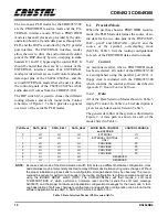
When the user has chosen a PROVIDED resource
mode, the PLD Mode determines the source of au-
dio data for the two data pins of the DSP (CMP-
DAT—pin 27 and SDATAN1—pin 22) and the
source of the system's oversampling clock
(MCLK). Table 3 lists the routing configurations
for each of the PROVIDED data selection modes.
5.1.1
Control
As mentioned earlier, when a PROVIDED mode
has been selected, all control of the CDB4923/300
is accomplished using the parallel port (J29). A
floppy disk is included with the CDB4923/300
which contains the control software described in
Appendix F: Board Control Software.
5.1.2
Data
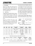
All of the Data Selection Modes shown in Table 3
imply PC control. In Table 4, a brief description is
given for each data source listed in Table 3.
The general data flow of the system is illustrated in
Figure 2. A data path is shown for each of the
modes listed in Table 3.
PLD Mode
DATA_SEL2
DATA_SEL1
DATA_SEL0
AUDIO DATA, CONTROL,
and CLOCKS
CONTROL SOURCE
0
LO
LO
LO
EXTERNAL
J11
1
LO
LO
HI
EXTERNAL CONTROL
ONLY
J11
2
LO
HI
LO
PROVIDED
PC
3
LO
HI
HI
PROVIDED
PC
4
HI
LO
LO
PROVIDED
PC
5
HI
LO
HI
PROVIDED
PC
6
HI
HI
LO
RESERVED
7
HI
HI
HI
RESERVED
NOTE: Because each mode of the Data Selection switch (S3) sets up a different hardware configuration, clock
and data lines may be momentarily directed to many different destinations during mode changes. Without
the proper initialization process after a reconfiguration, strange behavior may be observed. The recom-
mended procedure for performing changes to the routing configuration is to first generate a board reset
using the BOARD RESET switch (SW1). The CS492x/CS493xx will then require a soft reset
("CDB30RST.EXE -s" which performs a hardware reset and then sends the soft reset message
0x000001) and the proper hardware and application configuration messages for the new mode. A thor-
ough description of soft reset, hardware configuration, and application configuration can be found in the
software Application Notes AN115, AN120-123, AN140 or AN161-163.
Table 2. Data Selection Modes (PLD version AB-X)
Summary of Contents for CS492 Series
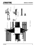
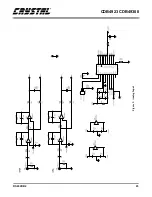
Page 18: ...CDB4923 CDB49300 18 DS262DB2 9 APPENDIX A SCHEMATICS Figure 4 CS492x CS493xx ...
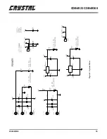
Page 19: ...CDB4923 CDB49300 DS262DB2 19 Figure 5 System Power ...
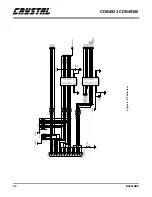
Page 20: ...CDB4923 CDB49300 20 DS262DB2 Figure 6 PC Interface ...
Page 21: ...CDB4923 CDB49300 DS262DB2 21 Figure 7 Control Logic ...
Page 22: ...CDB4923 CDB49300 22 DS262DB2 Figure 8 Clocking ...
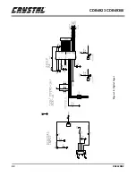
Page 23: ...CDB4923 CDB49300 DS262DB2 23 Figure 9 Analog Input ...
Page 24: ...CDB4923 CDB49300 24 DS262DB2 Figure 10 Digital Input ...
Page 25: ...CDB4923 CDB49300 DS262DB2 25 Figure 11 D A Converters ...
Page 26: ...CDB4923 CDB49300 26 DS262DB2 Figure 12 Analog Output ...
Page 27: ...CDB4923 CDB49300 DS262DB2 27 Figure 13 Digital Output ...
Page 28: ...CDB4923 CDB49300 28 DS262DB2 Figure 14 Top Layer ...
Page 29: ...CDB4923 CDB49300 DS262DB2 29 Figure 15 Bottom Layer ...
Page 30: ...CDB4923 CDB49300 30 DS262DB2 Figure 16 SSTOP ...
Page 31: ...CDB4923 CDB49300 DS262DB2 31 Figure 17 ASYSTOP ...
Page 32: ...CDB4923 CDB49300 32 DS262DB2 Figure 18 Layer 2 ...
Page 33: ...CDB4923 CDB49300 DS262DB2 33 Figure 19 Layer 3 ...
Page 49: ... Notes ...
Page 50: ......


