CDB4923 CDB49300
DS262DB2
43
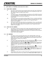
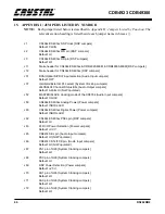
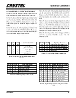
14. APPENDIX H: JUMPERS LISTED BY FUNCTION
14.1
AUDIO INPUT JUMPERS
J31
This jumper is used to select the input connector which is being used to receive S/PDIF data.
Placing the jumper in the ’RCA’ position enables the RCA jack, and placing the jumper in the
’OPT’ position enables the TORX173 optical receiver.
Default: OPT
J52
This jumper is used to control the MASTER/SLAVE clocking mode of the CS5334 as described
in the CS5334 datasheet. This jumper should be left in the ’SLAVE’ position when using the fac-
tory programmed PLD provided with the CDB4923/300.
Default: SLAVE
J65
This jumper is used to control the SEL pin of the CS8414. This pin, in conjunction with J66, is
used to select which channel status pin information to display on the status output pins. Please
refer to the CS8414 datasheet for more details on how to configure the CS8414.
Default: HI (Not Populated).
J66
This jumper is used to control the CS12/FCK pin of the CS8414. This pin, in conjunction with
J65, is used to select which channel status pin information to display on the status output pins.
Please refer to the CS8414 datasheet for more details on how to configure the CS8414.
Default: HI (Not Populated).
14.2
AUDIO OUTPUT JUMPERS
J44
This particular component is actually a set of jumpers. Each individual jumper can be used to
control the state of one channel status bit in the outgoing S/PDIF stream created by the
CS8404A. More details can be found in the datasheet for the CS8404A and the specifications
for IEC60958 and IEC61937 bitstreams.
Default: All bits HI {Not Populated}
14.3
DSP JUMPERS
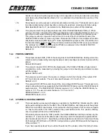
J1
This jumper is used to control the internal clocking of the CS492x/CS493xx. When in the
’CLKIN’ position, the CS492x/CS493xx uses the clock on the CLKIN pin to drive the DSP core
directly. When in the ’PLL’ position, the CS492x/CS493xx derives all internal clocks from the
reference frequency provided at the CLKIN pin.
Default: CLKIN
J2
This jumper selects the pull-up/pull-down state of the CS492x/CS493xx’s WR pin. This jumper
is used in conjunction with J3 and J62 to select the Host Interface Mode of the
CS492x/CS493xx when it comes out of reset. By default the CDB4923/300 is configured for I2C
serial communication. The settings for J2 (WR), J3 (RD) and J62 (PSEL) are detailed in the
CS4923/4/5/6/7/8/9 datasheet and the CS49300 datasheet.
Default: HI
J3
This jumper selects the pull-up/pull-down state of the CS492x/CS493xx’s RD pin. This jumper
is used in conjunction with J2 and J62 to select the Host Interface Mode of the
CS492x/CS493xx when it comes out of reset. By default the CDB4923/300 is configured for I
2
C
serial communication. The settings for J2 (WR), J3 (RD) and J62 (PSEL) are detailed in the
CS4923/4/5/6/7/8/9 datasheet and the CS49300 datasheet.
Default: LO
J11
Stake header providing some serial communication lines, and all general purpose I/O pins. This
header is also serves as the memory interface to the CRD4923_MEM/CDB49300_MEM. This
Summary of Contents for CS492 Series
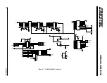
Page 18: ...CDB4923 CDB49300 18 DS262DB2 9 APPENDIX A SCHEMATICS Figure 4 CS492x CS493xx ...
Page 19: ...CDB4923 CDB49300 DS262DB2 19 Figure 5 System Power ...
Page 20: ...CDB4923 CDB49300 20 DS262DB2 Figure 6 PC Interface ...
Page 21: ...CDB4923 CDB49300 DS262DB2 21 Figure 7 Control Logic ...
Page 22: ...CDB4923 CDB49300 22 DS262DB2 Figure 8 Clocking ...
Page 23: ...CDB4923 CDB49300 DS262DB2 23 Figure 9 Analog Input ...
Page 24: ...CDB4923 CDB49300 24 DS262DB2 Figure 10 Digital Input ...
Page 25: ...CDB4923 CDB49300 DS262DB2 25 Figure 11 D A Converters ...
Page 26: ...CDB4923 CDB49300 26 DS262DB2 Figure 12 Analog Output ...
Page 27: ...CDB4923 CDB49300 DS262DB2 27 Figure 13 Digital Output ...
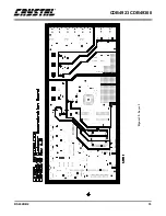
Page 28: ...CDB4923 CDB49300 28 DS262DB2 Figure 14 Top Layer ...
Page 29: ...CDB4923 CDB49300 DS262DB2 29 Figure 15 Bottom Layer ...
Page 30: ...CDB4923 CDB49300 30 DS262DB2 Figure 16 SSTOP ...
Page 31: ...CDB4923 CDB49300 DS262DB2 31 Figure 17 ASYSTOP ...
Page 32: ...CDB4923 CDB49300 32 DS262DB2 Figure 18 Layer 2 ...
Page 33: ...CDB4923 CDB49300 DS262DB2 33 Figure 19 Layer 3 ...
Page 49: ... Notes ...
Page 50: ......


