CDB4923 CDB49300
DS262DB2
11
CS5334
CS8414
Data
Parallel Compressed Data
Stereo PCM
C
S
8414
CS4340
CS4340
CS4340
CS8404A
CS8404A
CS8404A
CDI
DAI
PCM Out
XMT958
XM
T9
5
8
CS492x
CS493x
x
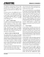
Figure 2. CDB4923/300 Data Paths
PLD
Mode
DATA_SEL2
DATA_SEL1
DATA_SEL0
CS492x/CS493xx
CMPDAT
CS492x/CS493xx
SDATAN1
MCLK
SOURCE
2
LO
HI
LO
PC
A/D — CS5334
DSP
3
LO
HI
HI
S/PDIF — CS8414
S/PDIF — CS8414
CS8414
4
HI
LO
LO
S/PDIF — CS8414
A/D — CS5334
CS8414
5
HI
LO
HI
A/D — CS5334
A/D — CS5334
OSC/PLL
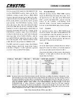
Table 3. PROVIDED Data Selection Modes (PLD version AB-X)
Digital Audio Source
Description
S/PDIF - CS8414
The CS8414 (U13) delivers the payload from an IEC60958 (linear PCM) or IEC61937 (nonlinear
PCM) encoded bit-stream. The incoming S/PDIF stream is connected to either J32 or J30.
A/D - CS5334
The CS5334 (U25) delivers stereo PCM which has been encoded from the analog input signals on
J55 and J56.
PC
A compressed digital audio stream is delivered in bursty format to the parallel port of the
CS492x/CS493xx from a file on the PC. This transfer mode requires that the CDB4923/300 is in a
parallel communication mode, and the PARLLPLY.EXE program is then used to deliver com-
pressed data through the PC interface.
NOTE: This data source is valid only for compressed audio and can be used only with parallel
communication modes (i.e. INTEL or Motorola mode).
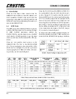
Table 4. Digital Audio Sources
Summary of Contents for CS492 Series
Page 18: ...CDB4923 CDB49300 18 DS262DB2 9 APPENDIX A SCHEMATICS Figure 4 CS492x CS493xx ...
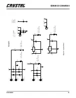
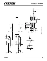
Page 19: ...CDB4923 CDB49300 DS262DB2 19 Figure 5 System Power ...
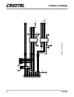
Page 20: ...CDB4923 CDB49300 20 DS262DB2 Figure 6 PC Interface ...
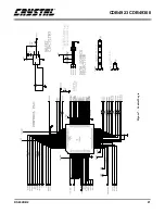
Page 21: ...CDB4923 CDB49300 DS262DB2 21 Figure 7 Control Logic ...
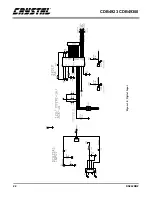
Page 22: ...CDB4923 CDB49300 22 DS262DB2 Figure 8 Clocking ...
Page 23: ...CDB4923 CDB49300 DS262DB2 23 Figure 9 Analog Input ...
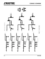
Page 24: ...CDB4923 CDB49300 24 DS262DB2 Figure 10 Digital Input ...
Page 25: ...CDB4923 CDB49300 DS262DB2 25 Figure 11 D A Converters ...
Page 26: ...CDB4923 CDB49300 26 DS262DB2 Figure 12 Analog Output ...
Page 27: ...CDB4923 CDB49300 DS262DB2 27 Figure 13 Digital Output ...
Page 28: ...CDB4923 CDB49300 28 DS262DB2 Figure 14 Top Layer ...
Page 29: ...CDB4923 CDB49300 DS262DB2 29 Figure 15 Bottom Layer ...
Page 30: ...CDB4923 CDB49300 30 DS262DB2 Figure 16 SSTOP ...
Page 31: ...CDB4923 CDB49300 DS262DB2 31 Figure 17 ASYSTOP ...
Page 32: ...CDB4923 CDB49300 32 DS262DB2 Figure 18 Layer 2 ...
Page 33: ...CDB4923 CDB49300 DS262DB2 33 Figure 19 Layer 3 ...
Page 49: ... Notes ...
Page 50: ......


