CDB4923 CDB49300
12
DS262DB2
5.1.3
Audio Clocking
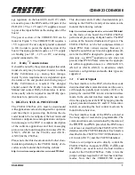
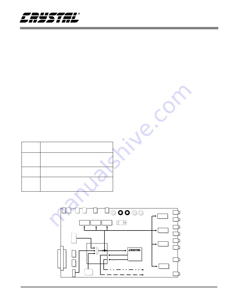
The audio clocking scheme is illustrated below in
Figure 3. Note that MCLK is bidirectional with re-
spect to the DSP. When the DSP is slaved to an ex-
ternal MCLK, i.e. the MCLK source is not listed as
DSP, the DSP will slave to the MCLK of the
CS8414 or the MCLK derived from the on-board
PLL (U26) or the OSCILLATOR (Y1). When the
internal PLL of the CS492x/CS493xx is being
used, however, the DSP will master the MCLK.
Caution must be observed when choosing a partic-
ular data selection mode and configuring the DSP
to ensure that there is no contention with the PLD
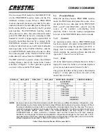
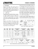
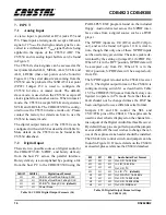
(U11). Each PLD mode given in Table 3 lists the
associated MCLK master - this table should be ref-
erenced whenever reconfiguring the
CDB4923/300. A brief description of each MCLK
source is given in Table 5.
5.2
External Mode
The EXTERNAL mode is designed to allow users
to drive the DSP directly with an external micro-
controller. Stake headers J11 and J12 contain all of
the signals required for host communication with
the CS492x/CS493xx. When operating in this
mode the DSP control pins are tri-stated by the
PLD (U11), effectively disabling the PC interface.
Consequently, the software bundled with the demo
board will not be functional.
The main DSP clock is always provided by the
CDB4923/300 (please see the Clocking section to
determine how to select the oscillator or external
PLL), and the output signals AUDATA0-2 are still
routed to the CS8404A S/PDIF transmitters and
CS4340 DACs.
Depending on the EXTERNAL mode selected the
user may be responsible for all data, control, and
clock signals going to the DSP, or just control.
NOTE: ALL SIGNALS DRIVEN TO THE CS493xx
MUST BE +3.3 V LOGIC. Because the
CS493xx does not have +5 V tolerant pads, an
external buffer such as the 74VHC244 should
be used for level conversion of any signals driv-
en to the DSP. Failure to 5 V signals
can cause permanent damage to the DSP. If
necessary, level shifting buffers can be wired
into the digital patch area of the CDB49300.
MCLK
Source
Description
CS8414
The CS8414 (U13) derives the sampling fre-
quency (Fs) from an incoming S/PDIF stream
and masters a 256 Fs MCLK
DSP
The DSP (U1) masters MCLK, generally when
using broadcast application code
OSC/PLL
The source of the main DSP clock also sup-
plies the system 256 Fs MCLK (see Clocking
for details)
Table 5. Clocking Descriptions
CS5334
CS492x
CS493xx
CS8414 MCLK
CS
8414
CS4340
CS4340
CS4340
CS8404A
CS8404A
CS8404A
DIGITAL MCLK / ANALOG MCLK
DSP MCLK
OSC
PL
L
DSP SCLK
DSP LRCLK
DIGITAL SCLK / ANALOG SCLK
DIGITAL LRCLK / ANALOG LRCLK
Figure 3. Audio Clocking
Summary of Contents for CS492 Series
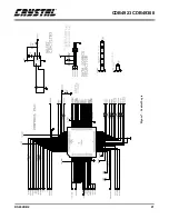
Page 18: ...CDB4923 CDB49300 18 DS262DB2 9 APPENDIX A SCHEMATICS Figure 4 CS492x CS493xx ...
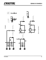
Page 19: ...CDB4923 CDB49300 DS262DB2 19 Figure 5 System Power ...
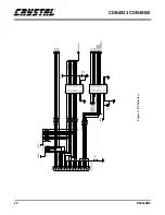
Page 20: ...CDB4923 CDB49300 20 DS262DB2 Figure 6 PC Interface ...
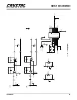
Page 21: ...CDB4923 CDB49300 DS262DB2 21 Figure 7 Control Logic ...
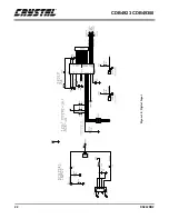
Page 22: ...CDB4923 CDB49300 22 DS262DB2 Figure 8 Clocking ...
Page 23: ...CDB4923 CDB49300 DS262DB2 23 Figure 9 Analog Input ...
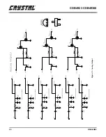
Page 24: ...CDB4923 CDB49300 24 DS262DB2 Figure 10 Digital Input ...
Page 25: ...CDB4923 CDB49300 DS262DB2 25 Figure 11 D A Converters ...
Page 26: ...CDB4923 CDB49300 26 DS262DB2 Figure 12 Analog Output ...
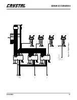
Page 27: ...CDB4923 CDB49300 DS262DB2 27 Figure 13 Digital Output ...
Page 28: ...CDB4923 CDB49300 28 DS262DB2 Figure 14 Top Layer ...
Page 29: ...CDB4923 CDB49300 DS262DB2 29 Figure 15 Bottom Layer ...
Page 30: ...CDB4923 CDB49300 30 DS262DB2 Figure 16 SSTOP ...
Page 31: ...CDB4923 CDB49300 DS262DB2 31 Figure 17 ASYSTOP ...
Page 32: ...CDB4923 CDB49300 32 DS262DB2 Figure 18 Layer 2 ...
Page 33: ...CDB4923 CDB49300 DS262DB2 33 Figure 19 Layer 3 ...
Page 49: ... Notes ...
Page 50: ......


