CDB4923 CDB49300
DS262DB2
15
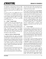
ally, both jumpers of J37 should be set to the OSC
position. In this clocking configuration you should
not use any modes which list OSC/PLL as the
MCLK source while Y1 is 27 MHz.
In order to use the 12.288 MHz oscillator directly,
Y1 should be populated with the 12.288 MHz os-
cillator included with the CDB4923/300 package,
and both jumpers of J37 should be set to the OSC
position. The 12.288 MHz oscillator can be used
with those PLD modes naming OSC/PLL as the
MCLK source, as 12.288 MHz is a standard 256Fs
oversampling frequency (256 * 48 kHz).
The choice of 12.288 MHz or 27 MHz is applica-
tion code dependent. Applications dealing with
IEC61937 packed compressed audio generally re-
quire a 12.288 MHz input, while broadcast applica-
tions typically require a 27 MHz input. Check the
relevant application code user’s guide (AN120-
AN123, AN140 or AN161-AN163) for details on
DSP CLKIN frequency.
If the external PLL is to be used, then Y1 must be
populated with a 27 MHz oscillator. The jumpers
of J37 should both be placed in the PLL position.
The CLKIN pin of the DSP will now be driven with
the processor clock (PCLK) output of U26. The
processor clock (PCLK) output can be configured
to generate either a many different frequencies,
based upon the configuration of jumpers J67, J68,
and J72 as listed in Table 12.
When using the external PLL to generate the DSP
clock, the CLKSEL pin (J1) of the
CS492x/CS493xx is typically set to ‘EXT CLK’.
6.2
MCLK
The system MCLK on the CDB4923/300 can come
from four different sources when using a PROVID-
ED mode. Some PLD modes use the MCLK gener-
ated by the CS8414 S/PDIF receiver (U13) when
there is an incoming S/PDIF stream. In PLD mode
2, the DSP generates MCLK when it is decoding a
compressed bit stream delivered by the PC. Some
modes can select between an MCLK which is sim-
ply the frequency of the on-board oscillator (Y1),
or a programmable MCLK generated by the exter-
nal PLL (U26).
The source of MCLK is dependent upon the PLD
mode and is indicated by the ‘MCLK SOURCE’
column of Table 9 and Table 24.
U26 is a discrete PLL which can generate many
different audio frequencies in addition to the pro-
cessor clock discussed above. The frequency of the
audio clock is controlled by the states of the AS1
and AS0 pins which are set with jumpers J70 and
J71. The available audio clock frequencies can be
used to support many different sampling frequen-
cies, depending on the desired MCLK ratio. Table
13 enumerates all possible MCLK frequencies for
the external PLL.
6.3
LRCLK and SCLK
LRCLK and SCLK are assumed to be generated by
the DSP in all cases. The audio clocking diagram
shown in Figure 3, illustrates the clocking scheme
of the CDB4923/300. If it is necessary to provide a
complete slave mode for the DSP, please contact
the factory for details on how to properly configure
the CDB4923/300.
PCLK Frequency
J72
J67
J68
33.33 MHz
LO
LO
LO
54 MHz
LO
LO
HI
66.66 MHz
LO
HI
LO
80 MHz
LO
HI
HI
32 MHz
HI
LO
LO
81 MHz
HI
LO
HI
50 MHz
HI
HI
LO
40 MHz
HI
HI
HI
Table 12. PCLK Configurations
MCLK Frequency
AS1 (J70)
AS0 (J71)
24.576 MHz
1
1
12.288 MHz
0
0
11.2896 MHz
0
1
8.192 MHz
1
0
Table 13. Audio Frequency Selection (J58)
Summary of Contents for CS492 Series
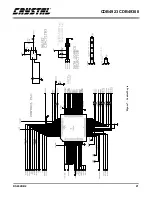
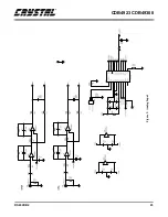
Page 18: ...CDB4923 CDB49300 18 DS262DB2 9 APPENDIX A SCHEMATICS Figure 4 CS492x CS493xx ...
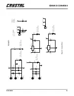
Page 19: ...CDB4923 CDB49300 DS262DB2 19 Figure 5 System Power ...
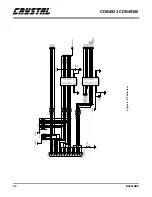
Page 20: ...CDB4923 CDB49300 20 DS262DB2 Figure 6 PC Interface ...
Page 21: ...CDB4923 CDB49300 DS262DB2 21 Figure 7 Control Logic ...
Page 22: ...CDB4923 CDB49300 22 DS262DB2 Figure 8 Clocking ...
Page 23: ...CDB4923 CDB49300 DS262DB2 23 Figure 9 Analog Input ...
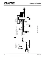
Page 24: ...CDB4923 CDB49300 24 DS262DB2 Figure 10 Digital Input ...
Page 25: ...CDB4923 CDB49300 DS262DB2 25 Figure 11 D A Converters ...
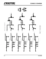
Page 26: ...CDB4923 CDB49300 26 DS262DB2 Figure 12 Analog Output ...
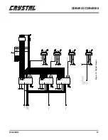
Page 27: ...CDB4923 CDB49300 DS262DB2 27 Figure 13 Digital Output ...
Page 28: ...CDB4923 CDB49300 28 DS262DB2 Figure 14 Top Layer ...
Page 29: ...CDB4923 CDB49300 DS262DB2 29 Figure 15 Bottom Layer ...
Page 30: ...CDB4923 CDB49300 30 DS262DB2 Figure 16 SSTOP ...
Page 31: ...CDB4923 CDB49300 DS262DB2 31 Figure 17 ASYSTOP ...
Page 32: ...CDB4923 CDB49300 32 DS262DB2 Figure 18 Layer 2 ...
Page 33: ...CDB4923 CDB49300 DS262DB2 33 Figure 19 Layer 3 ...
Page 49: ... Notes ...
Page 50: ......


