CDB4923 CDB49300
DS262DB2
17
8. OUTPUT
8.1
Analog Output
The six discrete outputs provided on the
CDB4923/300 are driven by CS4340 D/A convert-
ers. They can be found at RCA jacks J13-J16, J18,
and J20. Each output is driven directly by the
CS4340 to provide a 3.5 V
pp
full scale output. The
CS4340 and its control signals can be found in Fig-
ure 11, and the analog output buffers can be found
in Figure 12.
The digital input format of the CS4340 is config-
ured using switch S4. The CDB4923/300 is
shipped with the CS4340 in I
2
S mode, and should
not be changed unless the CS492x/CS493xx has
been configured to use a different serial format.
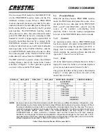
The list of data formats for the CS4340 can be
found in Table 16. For more details on the features
of the CS4340, please reference the CS4340
datasheet.
8.2
Analog Output Protection Circuitry
The CS4340 is designed to perform a ‘soft’ ramp-
ing of the bias voltage in order to prevent popping
on the outputs. However, the series capacitance
found in the analog buffers of the CS4340 require a
finite amount of time to discharge when the
CS4340 goes into reset (RC time constant). If the
full reset period is not observed before new audio is
delivered, popping can occur on the outputs. Please
see the CS4340 datasheet for more details.
The four transistors connected to the mute output of
each CS4340 are used to ensure that no 'popping'
will occur on the outputs during power-up, power-
down, and during audio clock discontinuities if the
reset period is violated.
8.3
Digital Output
The signals present on analog outputs J13-J16, J18,
and J20 can also be found on the digital outputs
J45-J47 (AOUTDIG0-AOUTDIG2). The optical
transmitters are driven by CS8404A S/PDIF trans-
mitters (U19-21). The CS8404As are configured to
operate in consumer mode by default. The mode of
operation and status bits can be controlled by in-
stalling a 16 pin header in J44 and placing jumpers
on the signals that are to be programmed low. All
signals on J44 are pulled up by default. The
CS8404A transmitters and optical outputs can be
found in Figure 13.
The digital input format of the S/PDIF transmitters
can be controlled with switch S2 as listed in
Table 17. More operational details for the
CS8404A can be found in the CS8404A datasheet.
Optical transmitter J43 (XMT958) is directly con-
nected to the S/PDIF transmitter of the DSP. It can
be used to directly observe the digital output of the
CS492x/CS493xx when the application code run-
ning on the part utilizes the transmitter. Note that if
the application code does not support S/PDIF trans-
mission, J43 will not generate valid data. Please see
the application note associated with the code in
question (e.g. AN120-123, AN140, or AN161-
AN163) to determine whether J43 should be active.
27DIF1
27DIF0
Digital Input Format
LO
LO
16-24 Bit I
2
S (default)
LO
HI
16-24 Bit Left Justified
HI
LO
24-Bit Right Justified
HI
HI
16-Bit Right Justified
Table 16. CS4340 Digital Input Formats (S4)
M2
M1
M0
Audio Serial Port Format
LO
LO
LO
FSYNC & SCK Output
LO
LO
HI
Left/Right, 16-24 Bits
LO
HI
LO
Word Sync, 16-24 Bits
LO
HI
HI
Reserved
HI
LO
LO
Left/Right, I
2
S (default)
HI
LO
HI
LSB Justified, 16 Bits
HI
HI
LO
LSB Justified, 18 Bits
HI
HI
1
MSB Last, 16-24 Bits
Table 17. Digital Input Format settings
for CS8404A (S2)
Summary of Contents for CS492 Series
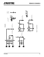
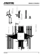
Page 18: ...CDB4923 CDB49300 18 DS262DB2 9 APPENDIX A SCHEMATICS Figure 4 CS492x CS493xx ...
Page 19: ...CDB4923 CDB49300 DS262DB2 19 Figure 5 System Power ...
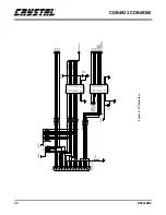
Page 20: ...CDB4923 CDB49300 20 DS262DB2 Figure 6 PC Interface ...
Page 21: ...CDB4923 CDB49300 DS262DB2 21 Figure 7 Control Logic ...
Page 22: ...CDB4923 CDB49300 22 DS262DB2 Figure 8 Clocking ...
Page 23: ...CDB4923 CDB49300 DS262DB2 23 Figure 9 Analog Input ...
Page 24: ...CDB4923 CDB49300 24 DS262DB2 Figure 10 Digital Input ...
Page 25: ...CDB4923 CDB49300 DS262DB2 25 Figure 11 D A Converters ...
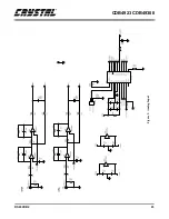
Page 26: ...CDB4923 CDB49300 26 DS262DB2 Figure 12 Analog Output ...
Page 27: ...CDB4923 CDB49300 DS262DB2 27 Figure 13 Digital Output ...
Page 28: ...CDB4923 CDB49300 28 DS262DB2 Figure 14 Top Layer ...
Page 29: ...CDB4923 CDB49300 DS262DB2 29 Figure 15 Bottom Layer ...
Page 30: ...CDB4923 CDB49300 30 DS262DB2 Figure 16 SSTOP ...
Page 31: ...CDB4923 CDB49300 DS262DB2 31 Figure 17 ASYSTOP ...
Page 32: ...CDB4923 CDB49300 32 DS262DB2 Figure 18 Layer 2 ...
Page 33: ...CDB4923 CDB49300 DS262DB2 33 Figure 19 Layer 3 ...
Page 49: ... Notes ...
Page 50: ......

