CDB4923 CDB49300
44
DS262DB2
header can be used to probe signals during normal operation, and may be used as a wirewrap
point when using Data Selection Mode 0 or 1, as detailed in the Data Selection section of this
datasheet.
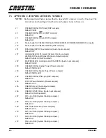
J12
Stake header providing access to all serial audio data and clock pins. This header can be used
to probe signals during normal operation, and may be used as a wirewrap point when using
Data Selection Mode 0 or 1, as detailed in the Data Selection section of this datasheet
J62
This jumper selects the pull-up/pull-down state of the CS492x/CS493xx’s PSEL pin. When
coming out of reset, the state of the PSEL pin determines which parallel interface mode to use
(Motorola or Intel) when initializing the CS492x/CS493xx into a parallel host interface mode.
This jumper is used in conjunction with J2 and J3 to select the Host Interface Mode of the
CS492x/CS493xx when it comes out of reset. Because the PSEL pin has multiplexed function-
ality it also serves as SCDIO when in I
2
C mode. By default this jumper is in the ’HI’ position since
the board is initially configured for I
2
C serial communication and the SCDIO pin is open-drained.
The settings for J2 (WR), J3 (RD) and J62 (PSEL) are detailed in the CS4923/4/5/6/7/8/9
datasheet and the CS49300 datasheet.
Default: HI
14.4
POWER JUMPERS
J59
This jumper connects DSP_PWR to the analog side of the CS492x/CS493xx. Analog current con-
sumption can be measured by removing this jumper and connecting an ammeter in series with the
jumper.
Default: INSTALLED
J60
This jumper connects DSP_PWR to the digital side of the CS492x/CS493xx. Digital current
consumption can be measured by removing this jumper and connecting an ammeter in series
with the jumper.
Default: INSTALLED
J63
This jumper is used to select the maximum voltage at which the I/O pins of the system PLD
(U11) will drive its outputs. The user can select b3.3 V and +2.5 V.
Default: +3.3 V
J69
This jumper (DSP_PWR) is used to select the core voltage for DSP power. This jumper is pro-
vided to allow the user to evaluate both the CS4923/4/5/6/7/8 family and the CS49300 family of
audio decoders. The CS4923/4/5/6/7/8 family re3.3 V, while the CS49300 family re-
2.5 V. The user can select b3.3 V and +2.5 V.
CDB4923 Default: +3.3 V
CDB49300 Default: +2.5 V
14.5
SYSTEM CLOCKING JUMPERS
J37
This dual position jumper select between an oscillator or the MK2744-10S discrete PLL (U26)
as the external clock source for the DSP of the CS492x/CS493xx, and it also selects the system
MCLK for non-S/PDIF input modes. It is important to note the jumpers of J37 must move togeth-
er. They must be both in the ’OSC’ position or they must both be in the ’PLL’ position. Moving
only one jumper will result in erratic behavior.
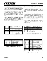
When both jumpers are in the ’OSC’ position, the CS492x/CS493xx CLKIN pin is driven by the
oscillator, Y1, and some of the data modes chosen by switch S3 will provide a system MCLK
which is also derived from Y1. Specifically, all data selection modes listed in Table 9 and Table
24 showing an MCLK Source of ’OSC/PLL’ will generate a system MCLK equal to the frequency
of the oscillator Y1.
If you have questions about how to utilize the external PLL, please contact the factory before
Summary of Contents for CS492 Series
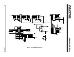
Page 18: ...CDB4923 CDB49300 18 DS262DB2 9 APPENDIX A SCHEMATICS Figure 4 CS492x CS493xx ...
Page 19: ...CDB4923 CDB49300 DS262DB2 19 Figure 5 System Power ...
Page 20: ...CDB4923 CDB49300 20 DS262DB2 Figure 6 PC Interface ...
Page 21: ...CDB4923 CDB49300 DS262DB2 21 Figure 7 Control Logic ...
Page 22: ...CDB4923 CDB49300 22 DS262DB2 Figure 8 Clocking ...
Page 23: ...CDB4923 CDB49300 DS262DB2 23 Figure 9 Analog Input ...
Page 24: ...CDB4923 CDB49300 24 DS262DB2 Figure 10 Digital Input ...
Page 25: ...CDB4923 CDB49300 DS262DB2 25 Figure 11 D A Converters ...
Page 26: ...CDB4923 CDB49300 26 DS262DB2 Figure 12 Analog Output ...
Page 27: ...CDB4923 CDB49300 DS262DB2 27 Figure 13 Digital Output ...
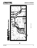
Page 28: ...CDB4923 CDB49300 28 DS262DB2 Figure 14 Top Layer ...
Page 29: ...CDB4923 CDB49300 DS262DB2 29 Figure 15 Bottom Layer ...
Page 30: ...CDB4923 CDB49300 30 DS262DB2 Figure 16 SSTOP ...
Page 31: ...CDB4923 CDB49300 DS262DB2 31 Figure 17 ASYSTOP ...
Page 32: ...CDB4923 CDB49300 32 DS262DB2 Figure 18 Layer 2 ...
Page 33: ...CDB4923 CDB49300 DS262DB2 33 Figure 19 Layer 3 ...
Page 49: ... Notes ...
Page 50: ......


