DS785UM1
7-33
Copyright 2007 Cirrus Logic
Raster Engine With Analog/LCD Integrated Timing and Interface
EP93xx User’s Guide
7
7
7
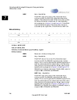
7.4.11.2.1 PattrnMask Register
This register defines which bits in a pixel are blink bits. To enable an individual bit for
comparison requires setting that corresponding bit to “1”. To disable an individual bit for
comparison set the bit position to “0”.
For example, in 8bpp mode, the PattrnMask is defined as 0x0000_0080. This means that the
MSB of a pixel is used to assist is defined as a blink bit.
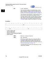
7.4.11.2.2 BlinkPattrn Register
The
register is used to further refine which pixel pattern defines a blink pixel.
The pixel value is first masked by the PattrnMask value in the
register and the
result is compared to BlinkPattrn value in the
register. If the comparison results
in a match, the pixel is considered to be a valid blink pixel.
For example:
An 8-bit pixel is defined as 0xAF (0b1010_1111b).
PattrnMask is defined as 0x0000_00C0.
BlinkPattrn is defined as 0x0000_0080.
PattrnMask = 0xC0 defines the two MSBs of 8-bit pixels as potential blink bits. If the two
corresponding MSBs in the BlinkPattrn register are ‘10’ and the two MSBs of the pixel value
are ‘10’, then the pixel of value = 0xAF is a blink pixel. In fact, all pixel values of 10xx_xxxx
are blink pixels. If BlinkPattrn was changed to 0x0000_0048 above, a pixel of value 0xAF
would not be a blink pixel.
7.4.11.2.3 BlinkMask Register
The
register is only used if the blink mode definition bits M[3:0] in the
register are set for an AND, OR, or XOR operation. The value in the
register is ANDed (clearing bits), ORed (setting bits), or XORed (inverting bits) with a pixel
that addresses the LUT. The mask allows a blinking pixel to jump from a normal color
definition location to a blink color definition location in the LUT.
7.4.11.3 Types of Blinking
Once a pixel has been defined as a blink pixel, it is necessary to provide information on how
that pixel will blink. The blink type provides determines what operations are performed on the
pixel data as it moves through the blink logic to transform it into a blinking pixel.
There are 10 ways to blink a pixel once it has been defined as a blinking pixel. The blink type
is defined by the M[3:0] bits in the
register:
0000 - Blink Disabled
0001 - AND Blinking.
The pixel data is ANDed with the
register. The modified pixel data will
continue through the pipeline.
LUT Blink:
Summary of Contents for EP93 Series
Page 28: ...P 6 DS785UM1 Copyright 2007 Cirrus Logic Preface EP93xx User s Guide PP P ...
Page 162: ...5 36 DS785UM1 Copyright 2007 Cirrus Logic System Controller EP93xx User s Guide 55 5 ...
Page 576: ...15 18 DS785UM1 Copyright 2007 Cirrus Logic UART2 EP93xx User s Guide 1515 15 ...
Page 634: ...17 38 DS785UM1 Copyright 2007 Cirrus Logic IrDA EP93xx User s Guide 1717 17 ...
Page 648: ...19 6 DS785UM1 Copyright 2007 Cirrus Logic Watchdog Timer EP93xx User s Guide 1919 19 ...
Page 688: ...21 32 DS785UM1 Copyright 2007 Cirrus Logic I2S Controller EP93xx User s Guide 2121 21 ...
Page 790: ...27 20 DS785UM1 Copyright 2007 Cirrus Logic IDE Interface EP93xx User s Guide 2727 27 ...
Page 808: ...28 18 DS785UM1 Copyright 2007 Cirrus Logic GPIO Interface EP93xx User s Guide 2828 28 ...


