DS785UM1
7-55
Copyright 2007 Cirrus Logic
Raster Engine With Analog/LCD Integrated Timing and Interface
EP93xx User’s Guide
7
7
7
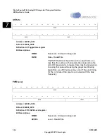
PCLKEN:
Pixel Clock Enable - Read/Write
The value written to this bit selects whether the pixel clock
or smart panel clock are output to the SPCLK pin, or not:
0 - SPCLK pin at high impedance
1 - PCLK or SCLK active on SPCLK pin
The PIFEN bit above selects PCLK vs. SCLK.
EN:
Enable Video State Machine - Read/Write
The value written to this bit selects whether the video state
machine is enabled, or not:
0 - Video state machine off
1 - Video state machine enabled
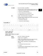
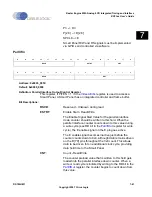
RasterSWLock
Address: 0x8003_007C
Default: 0x0000_0000
Definition: Raster Software Lock register
Bit Descriptions:
RSVD:
Reserved - Unknown during read
SWLCK:
Software Lock - Read/Write
WRITE: Writing 0X0000_00AA to this register will unlock
all locked registers until the next block access.
READ: During a read operation, SWLCK[0] has this
meaning:
1 - Unlocked for current bus access
0 - Locked
The Read feature of the RasterSWLock register is used for
testing the locking function.
31
30
29
28
27
26
25
24
23
22
21
20
19
18
17
16
RSVD
15
14
13
12
11
10
9
8
7
6
5
4
3
2
1
0
RSVD
SWLCK
Summary of Contents for EP93 Series
Page 28: ...P 6 DS785UM1 Copyright 2007 Cirrus Logic Preface EP93xx User s Guide PP P ...
Page 162: ...5 36 DS785UM1 Copyright 2007 Cirrus Logic System Controller EP93xx User s Guide 55 5 ...
Page 576: ...15 18 DS785UM1 Copyright 2007 Cirrus Logic UART2 EP93xx User s Guide 1515 15 ...
Page 634: ...17 38 DS785UM1 Copyright 2007 Cirrus Logic IrDA EP93xx User s Guide 1717 17 ...
Page 648: ...19 6 DS785UM1 Copyright 2007 Cirrus Logic Watchdog Timer EP93xx User s Guide 1919 19 ...
Page 688: ...21 32 DS785UM1 Copyright 2007 Cirrus Logic I2S Controller EP93xx User s Guide 2121 21 ...
Page 790: ...27 20 DS785UM1 Copyright 2007 Cirrus Logic IDE Interface EP93xx User s Guide 2727 27 ...
Page 808: ...28 18 DS785UM1 Copyright 2007 Cirrus Logic GPIO Interface EP93xx User s Guide 2828 28 ...


