DS785UM1
23-11
Copyright 2007 Cirrus Logic
Synchronous Serial Port
EP93xx User’s Guide
2
3
2
3
23
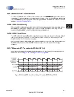
Microwire format is very similar to SPI format, except that transmission is half-duplex instead
of full-duplex, using a master-slave message passing technique. Each serial transmission
begins with an 8-bit control word that is transmitted from the SSP to the off-chip slave device.
During this transmission, no incoming data is received by the SSP. After the message has
been sent, the off-chip slave decodes it and, after waiting one serial clock after the last bit of
the 8-bit control message has been sent, responds with the required data. The returned data
is 4 to 16 bits in length, making the total frame length anywhere from 13 to 25 bits.
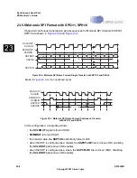
In this configuration, during idle periods:
•
the SCLKOUT signal is forced LOW
•
SFRMOUT is forced HIGH
•
the transmit data line SSPTXD is arbitrarily forced LOW
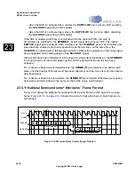
A transmission is triggered by writing a control byte to the transmit FIFO. The falling edge of
SFRMOUT causes the value contained in the bottom entry of the transmit FIFO to be
transferred to the serial shift register of the transmit logic, and the MSB of the 8-bit control
frame to be shifted out onto the SSPTXD pin. SFRMOUT remains LOW for the duration of the
frame transmission. The SSPRXD pin remains in a high impedance state during this
transmission.
The off-chip serial slave device latches each control bit into its serial shifter on the rising edge
of each SCLKOUT. After the last bit is latched by the slave device, the control byte is
decoded during a one clock wait-state, and the slave responds by transmitting data back to
the SSP. Each bit is driven onto SSPRXD line on the falling edge of SCLKOUT. The SSP in
turn latches each bit on the rising edge of SCLKOUT. At the end of the frame, for single
transfers, the SFRMOUT signal is pulled HIGH one clock period after the last bit has been
latched in the receive serial shifter, that causes the data to be transferred to the receive FIFO.
Note: The off-chip slave device can put the receive line in a high impedance state either on the
falling edge of SCLKOUT after the LSB has been latched by the receive shifter, or when
the SFRMOUT pin goes HIGH.
For continuous transfers, data transmission begins and ends in the same manner as a single
transfer. However, the SFRMOUT line is continuously asserted (held LOW) and transmission
of data occurs back to back. The control byte of the next frame follows directly after the LSB
of the received data from the current frame. Each of the received values is transferred from
the receive shifter on the falling edge SCLKOUT, after the LSB of the frame has been latched
into the SSP.
Summary of Contents for EP93 Series
Page 28: ...P 6 DS785UM1 Copyright 2007 Cirrus Logic Preface EP93xx User s Guide PP P ...
Page 162: ...5 36 DS785UM1 Copyright 2007 Cirrus Logic System Controller EP93xx User s Guide 55 5 ...
Page 576: ...15 18 DS785UM1 Copyright 2007 Cirrus Logic UART2 EP93xx User s Guide 1515 15 ...
Page 634: ...17 38 DS785UM1 Copyright 2007 Cirrus Logic IrDA EP93xx User s Guide 1717 17 ...
Page 648: ...19 6 DS785UM1 Copyright 2007 Cirrus Logic Watchdog Timer EP93xx User s Guide 1919 19 ...
Page 688: ...21 32 DS785UM1 Copyright 2007 Cirrus Logic I2S Controller EP93xx User s Guide 2121 21 ...
Page 790: ...27 20 DS785UM1 Copyright 2007 Cirrus Logic IDE Interface EP93xx User s Guide 2727 27 ...
Page 808: ...28 18 DS785UM1 Copyright 2007 Cirrus Logic GPIO Interface EP93xx User s Guide 2828 28 ...

