27-12
DS785UM1
Copyright 2007 Cirrus Logic
IDE Interface
EP93xx User’s Guide
2
7
2
7
27
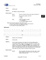
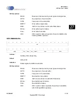
Note: At most, one of the above 3 bits should be set to 1 at any time. If more than one is set, the
results will be unpredictable, and the data invalid.
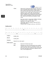
MODE:
Speed mode number. (0 to 4 defined for PIO, 0 to 2
defined for MDMA, 0 to 4 defined for UDMA).
WST:
Wait State for Turn. Number of HCLK cycles to hold the
data bus after a PIO write operation.
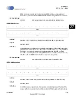
IDEMDMAOp
Address:
0x800A_0008 Read/Write
Default:
0x0000_0000
Definition:
IDE MDMA Configuration Register.
Bit Descriptions:
RSVD:
Reserved. Unknown during read, ignored during write.
MEN:
Enable Multiword DMA operation.
1 - to start MDMA
0 - to terminate MDMA by the host.
RWOP:
Read or write operation selection:
0 - Read
1 - Write.
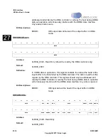
IDEUDMAOp
Address:
0x800A_000C - Read/Write
31
30
29
28
27
26
25
24
23
22
21
20
19
18
17
16
RSVD
15
14
13
12
11
10
9
8
7
6
5
4
3
2
1
0
RSVD
RWOP
MEN
31
30
29
28
27
26
25
24
23
22
21
20
19
18
17
16
RSVD
15
14
13
12
11
10
9
8
7
6
5
4
3
2
1
0
RSVD
RWOP
UEN
Summary of Contents for EP93 Series
Page 28: ...P 6 DS785UM1 Copyright 2007 Cirrus Logic Preface EP93xx User s Guide PP P ...
Page 162: ...5 36 DS785UM1 Copyright 2007 Cirrus Logic System Controller EP93xx User s Guide 55 5 ...
Page 576: ...15 18 DS785UM1 Copyright 2007 Cirrus Logic UART2 EP93xx User s Guide 1515 15 ...
Page 634: ...17 38 DS785UM1 Copyright 2007 Cirrus Logic IrDA EP93xx User s Guide 1717 17 ...
Page 648: ...19 6 DS785UM1 Copyright 2007 Cirrus Logic Watchdog Timer EP93xx User s Guide 1919 19 ...
Page 688: ...21 32 DS785UM1 Copyright 2007 Cirrus Logic I2S Controller EP93xx User s Guide 2121 21 ...
Page 790: ...27 20 DS785UM1 Copyright 2007 Cirrus Logic IDE Interface EP93xx User s Guide 2727 27 ...
Page 808: ...28 18 DS785UM1 Copyright 2007 Cirrus Logic GPIO Interface EP93xx User s Guide 2828 28 ...


