8-36
DS785UM1
Copyright 2007 Cirrus Logic
Graphics Accelerator
EP93xx User’s Guide
8
8
8
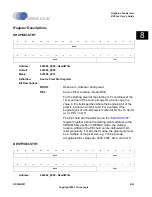
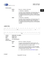
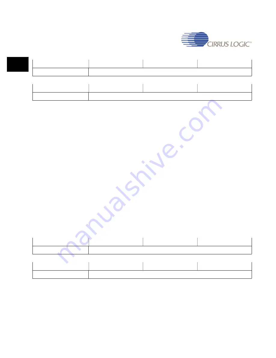
LINEINC
Address:
0x8004_00343 - Read/Write
Default:
0x0000_0000
Mask:
0x0FFF_0FFF
Definition:
Line Draw Increment Register
Bit Descriptions:
RSVD:
Reserved - Unknown during read
YINC:
Y Increment - Read/Write
The value in this field specifies a 12-bit binary fraction of a
pixel to be accumulated in the vertical (Y) direction during
a Line Draw function. The maximum value is 4095/4096
and the minimum value is 1/4096.
XINC:
X Increment - Read/Write
The value in this field specifies a 12 bit binary fraction of a
pixel to be accumulated in the horizontal (X) direction
during a Line Draw function. The maximum value is
4095/4096 and the minimum value is 1/4096.
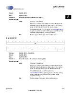
LINEINIT
Address:
0x8004_0038 - Read/Write
Default:
0x0000_0000
Mask:
0x0FFF_0FFF
Definition:
Line Draw Initialization Register
31
30
29
28
27
26
25
24
23
22
21
20
19
18
17
16
RSVD
YINC
15
14
13
12
11
10
9
8
7
6
5
4
3
2
1
0
RSVD
XINC
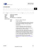
31
30
29
28
27
26
25
24
23
22
21
20
19
18
17
16
RSVD
YINIT
15
14
13
12
11
10
9
8
7
6
5
4
3
2
1
0
RSVD
XINIT
Summary of Contents for EP93 Series
Page 28: ...P 6 DS785UM1 Copyright 2007 Cirrus Logic Preface EP93xx User s Guide PP P ...
Page 162: ...5 36 DS785UM1 Copyright 2007 Cirrus Logic System Controller EP93xx User s Guide 55 5 ...
Page 576: ...15 18 DS785UM1 Copyright 2007 Cirrus Logic UART2 EP93xx User s Guide 1515 15 ...
Page 634: ...17 38 DS785UM1 Copyright 2007 Cirrus Logic IrDA EP93xx User s Guide 1717 17 ...
Page 648: ...19 6 DS785UM1 Copyright 2007 Cirrus Logic Watchdog Timer EP93xx User s Guide 1919 19 ...
Page 688: ...21 32 DS785UM1 Copyright 2007 Cirrus Logic I2S Controller EP93xx User s Guide 2121 21 ...
Page 790: ...27 20 DS785UM1 Copyright 2007 Cirrus Logic IDE Interface EP93xx User s Guide 2727 27 ...
Page 808: ...28 18 DS785UM1 Copyright 2007 Cirrus Logic GPIO Interface EP93xx User s Guide 2828 28 ...

