DS785UM1
13-3
Copyright 2007 Cirrus Logic
SDRAM, SyncROM, and SyncFLASH Controller
EP93xx User’s Guide
1
3
1
3
13
it’s data outputs in the high impedance state. If power-on reset has become de-
asserted, the ARM Core is released from the reset state.
13.3 Address Pin Usage
Each of the four synchronous memory domains can be fitted with a variety of device types,
provided the total capacitance on any address/control/data line does not exceed the specified
operating limit. Four pins, SDCSn[3:0], are used to as chip-selects (domain selects) for the
four synchronous memory domains, where the configurations of the domains are specified by
registers SDRAMDevCfg[3:0], SDRAMDevCfg[3:0], SDRAMDevCfg[3:0], and
SDRAMDevCfg[3:0], respectively. For example, SDCSn[2] selects the 3rd of four
synchronous memory domains and SDRAMDevCfg[3:0] specifies the configuration of that
domain.
Address bits 31:28 are internally decoded to specify an address domain.
shows
he values of address bits 31:28 that specify a synchronous memory domain.
Because of the row/column/bank architecture of synchronous memory devices, the mapping
of these memories into the processor’s memory space is not always obvious, typically
because the memory inside a synchronous device does not appear to the processor to be
continuous. For example, a 32-Mbyte SDRAM device may be visible as four 4-Mbyte banks.
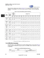
shows address pin usage. In
, external pins are identified as AD[15:0],
internal address signals are identified as A[27:1]. The 2nd row of the table shows the address
pins, AD[15:0], that may be connected to the synchronous memory device, depending on its
address depth. The remaining rows show how the device’s linear address space is mapped
onto the address pins, AD[15:0]. For each memory device configuration, that is, 16- or 32-bit
wide SDRAM or SROM or SFLASH, there is a Row and Bank, and Column, entry in the table
that shows the internal linear address bits, A[27:1], that are presented on the external
AD[15:0] pins for Row and Bank, and Column, accesses. The shallower the depth of the
synchronous memory device, the fewer the number of most-significant address bits that are
used for Row and Bank, and Column, addressing. By observing the number of rows and
columns in a specific synchronous memory device (see the device’s data sheet), the actual
number of address bits used for addressing the device can be determined. Because some
address bits are not used, the address map of the synchronous memory appears to be non-
continuous. The SROMLL should be used when possible to reduce the number of “holes” in
Table 13-2. Address Decoding for Synchronous Memory Domains
Value of Address
Bits 31:28
SDCSn[3:0]
Synchronous Memory Domain
0xF
3
4
0xE
2
3
0xD
1
2
0xC
0
1
0xB through 0x1
None
Used for other domains
0x0
3
Used during boot from SyncROM or
SyncFLASH
Summary of Contents for EP93 Series
Page 28: ...P 6 DS785UM1 Copyright 2007 Cirrus Logic Preface EP93xx User s Guide PP P ...
Page 162: ...5 36 DS785UM1 Copyright 2007 Cirrus Logic System Controller EP93xx User s Guide 55 5 ...
Page 576: ...15 18 DS785UM1 Copyright 2007 Cirrus Logic UART2 EP93xx User s Guide 1515 15 ...
Page 634: ...17 38 DS785UM1 Copyright 2007 Cirrus Logic IrDA EP93xx User s Guide 1717 17 ...
Page 648: ...19 6 DS785UM1 Copyright 2007 Cirrus Logic Watchdog Timer EP93xx User s Guide 1919 19 ...
Page 688: ...21 32 DS785UM1 Copyright 2007 Cirrus Logic I2S Controller EP93xx User s Guide 2121 21 ...
Page 790: ...27 20 DS785UM1 Copyright 2007 Cirrus Logic IDE Interface EP93xx User s Guide 2727 27 ...
Page 808: ...28 18 DS785UM1 Copyright 2007 Cirrus Logic GPIO Interface EP93xx User s Guide 2828 28 ...

