DS785UM1
13-9
Copyright 2007 Cirrus Logic
SDRAM, SyncROM, and SyncFLASH Controller
EP93xx User’s Guide
1
3
1
3
13
to the SyncFLASH register and the associated value on the data pins specifies which
SyncFLASH register is written. Actually, the value on the data pins specifies a command to
the SyncFLASH device such as Write Configuration Register, Lock Block, Block Erase; and
the associated value on the address pins specifies either a value that is written to a register
or a address location inside the SyncFLASH device.
Synchronous FLASH devices:
•
Use the same combination of the CS, RAS, CAS, and WE signals which would normally
place an SDRAM device into Auto-Refresh mode
•
Cannot be written in bursts, but only one word at a time. Hence the requirement to write
WBM = ‘1’ to the appropriate SDRAMDevCfg register. When WBM = ‘1’, no Auto
Refresh cycle will occur in the associated synchronous memory domain because the
synchronous memory controller will assume that a Synchronous FLASH device is
attached.
•
Require 100
μ
s of initialization time after a low-to-high transition occurs on its write
protect input pin
•
Can be set up by either programming the Synchronous FLASH Configuration register
before releasing the processor from reset or by using the contents of it’s
NonVolatileMODE register (which must have been previously programmed).
13.8 External Synchronous Memory System
The synchronous memory system is decoded from the ARM Core’s physical memory map
into four independent address domains, each having an address range of 256 Mbytes (64
Mwords). All of the memory devices that are attached to a given domain must be of the same
type, but the other domains may use different memory device types and associated timing
characteristics.
Since all memory devices, synchronous or static, share a common external memory bus, the
total number of devices is limited by the maximum allowable bus capacitance.
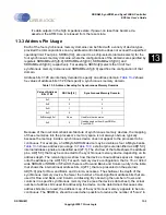
13.8.1 Chip Select SDCSN[3:0] Decoding
Each of the four address domains within synchronous memory space have an associated
chip select signal that is output on one of the SDCSn[3:0] pins as shown in
signals are decoded from address bits A31:A28.
The latched value of ASDO determines how SDCSn3 is mapped into synchronous memory
space. If the latched value of ASDO=1 then SDCSn3 is mapped to 0x0000_0000 otherwise it
is mapped to 0xF000_0000.
Table 13-9. Chip Select Decoding
Boot Option
(ASDO)
A31
A30
A29
A28
Chip select
1
0
0
0
0
nSDCS3
Summary of Contents for EP93 Series
Page 28: ...P 6 DS785UM1 Copyright 2007 Cirrus Logic Preface EP93xx User s Guide PP P ...
Page 162: ...5 36 DS785UM1 Copyright 2007 Cirrus Logic System Controller EP93xx User s Guide 55 5 ...
Page 576: ...15 18 DS785UM1 Copyright 2007 Cirrus Logic UART2 EP93xx User s Guide 1515 15 ...
Page 634: ...17 38 DS785UM1 Copyright 2007 Cirrus Logic IrDA EP93xx User s Guide 1717 17 ...
Page 648: ...19 6 DS785UM1 Copyright 2007 Cirrus Logic Watchdog Timer EP93xx User s Guide 1919 19 ...
Page 688: ...21 32 DS785UM1 Copyright 2007 Cirrus Logic I2S Controller EP93xx User s Guide 2121 21 ...
Page 790: ...27 20 DS785UM1 Copyright 2007 Cirrus Logic IDE Interface EP93xx User s Guide 2727 27 ...
Page 808: ...28 18 DS785UM1 Copyright 2007 Cirrus Logic GPIO Interface EP93xx User s Guide 2828 28 ...

