13-20
DS785UM1
Copyright 2007 Cirrus Logic
SDRAM, SyncROM, and SyncFLASH Controller
EP93xx User’s Guide
1
3
1
3
13
Writing a ‘1’ to this bit, in combination with the values of
the MRS and LCR bits, cause the Synchronous Memory
controller to issue either NOP or PreALL accesses to
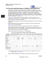
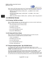
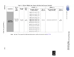
SDRAM devices as shown in
.
0 - See
1 - See
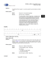
RefrshTimr
Address: 0x8006_0008 - Read/Write
Default: 0x0000_0080
Table 13-14. Synchronous Memory Command Encoding
Initialize
MRS
LCR
Synchronous Memory Command
1
1
0
Issue NOP to Synchronous Memory
1
0
0
Issue PreALL (Pre-charge All) to SDRAM
0
1
0
Enable access to Synchronous Memory device mode register
0
1
1
Issue command to Synchronous FLASH Memory devices
0
0
1
UNDEFINED. Do not use.
1
0
1
UNDEFINED. Do not use.
1
1
1
UNDEFINED. Do not use.
0
0
0
Normal operation
31
30
29
28
27
26
25
24
23
22
21
20
19
18
17
16
RSVD
15
14
13
12
11
10
9
8
7
6
5
4
3
2
1
0
Refcnt
Summary of Contents for EP93 Series
Page 28: ...P 6 DS785UM1 Copyright 2007 Cirrus Logic Preface EP93xx User s Guide PP P ...
Page 162: ...5 36 DS785UM1 Copyright 2007 Cirrus Logic System Controller EP93xx User s Guide 55 5 ...
Page 576: ...15 18 DS785UM1 Copyright 2007 Cirrus Logic UART2 EP93xx User s Guide 1515 15 ...
Page 634: ...17 38 DS785UM1 Copyright 2007 Cirrus Logic IrDA EP93xx User s Guide 1717 17 ...
Page 648: ...19 6 DS785UM1 Copyright 2007 Cirrus Logic Watchdog Timer EP93xx User s Guide 1919 19 ...
Page 688: ...21 32 DS785UM1 Copyright 2007 Cirrus Logic I2S Controller EP93xx User s Guide 2121 21 ...
Page 790: ...27 20 DS785UM1 Copyright 2007 Cirrus Logic IDE Interface EP93xx User s Guide 2727 27 ...
Page 808: ...28 18 DS785UM1 Copyright 2007 Cirrus Logic GPIO Interface EP93xx User s Guide 2828 28 ...

