DS785UM1
17-11
Copyright 2007 Cirrus Logic
IrDA
EP93xx User’s Guide
1
7
1
7
17
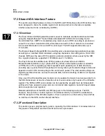
17.4.2 Functional Description
Following reset, the MIR is disabled. Reset also causes the transmit and receive buffers and
tail register to be flushed (buffers marked as empty). To transmit data in MIR mode, use the
following procedure:
1. Set the EN bits in the IrEnable register to 10b for MIR mode. Do not begin data
transmission.
2. Before enabling the MIR, the user must first clear any writable or “sticky” status bits that
are set by writing a one to each bit. (A sticky bit is a readable status bit that may be
cleared by writing a one to its location.) Set the TAB and TFC bits in the MISR register,
then read the MISR register to clear all interrupts.
3. Next, the desired mode of operation is programmed in the control register. Set the TXE
and RXE bits in the IrCtrl register.
4. Write 1 to 3 bytes to the appropriate IrDataTail register.
5. Once the MIR is enabled, transmission/reception of data can begin on the transmit and
receive pins.
17.4.2.1 Baud Rate Generation
The baud or bit rate is derived by dividing down an 18.423MHz clock. The clock is divided
down by either 1 (BRD=1) or 2 (BRD=0) and then by a fixed value of four, generating the
transmit clock for 1.152Mb/s and 0.576Mb/s data rates, respectively. The receive clock is
generated by the receiver Digital Phase Locked Loop (DPLL). The DPLL uses a sample clock
that is undivided. A sample rate counter (incremented at the sample clock rate) is used to
generate a receive clock at the nominal data rate (sample clock divided by 41 and two-thirds).
The sample rate counter is reset on the detection of each positive-going data transition
(indicating the RZI encoding of a “0”) to ensure that synchronization with the incoming data
stream is maintained.
17.4.2.2 Receive Operation
Once the MIR receiver is enabled it enters hunt mode, searching the incoming data stream
for the flag (01111110b). The flag serves to achieve bit synchronization, denotes the
beginning of a frame and delineates the boundaries of individual bytes of data. The end of the
second flag denotes the beginning of the address byte. Once the flag is found, the receiver is
synchronized to incoming data and hunt mode is exited.
After each bit is decoded, a serial shifter is used to receive the incoming data a byte at a time.
Once the flag is recognized, each subsequent byte of data is decoded and placed within a
two byte temporary buffer. A temporary buffer is used to prevent the CRC from being placed
within the receive buffer. When the temporary buffer is filled, data values are pushed out one
by one to the receive buffer. The first byte of a frame is the address. If receiver address
matching is enabled, the received address is compared to the address programmed in the
address match value field in a control register. If the two values are equal or if the incoming
address contains all ones, all subsequent data bytes including the address byte are stored in
the receive buffer. If the values do not match, the receive logic does not store any data in the
Summary of Contents for EP93 Series
Page 28: ...P 6 DS785UM1 Copyright 2007 Cirrus Logic Preface EP93xx User s Guide PP P ...
Page 162: ...5 36 DS785UM1 Copyright 2007 Cirrus Logic System Controller EP93xx User s Guide 55 5 ...
Page 576: ...15 18 DS785UM1 Copyright 2007 Cirrus Logic UART2 EP93xx User s Guide 1515 15 ...
Page 634: ...17 38 DS785UM1 Copyright 2007 Cirrus Logic IrDA EP93xx User s Guide 1717 17 ...
Page 648: ...19 6 DS785UM1 Copyright 2007 Cirrus Logic Watchdog Timer EP93xx User s Guide 1919 19 ...
Page 688: ...21 32 DS785UM1 Copyright 2007 Cirrus Logic I2S Controller EP93xx User s Guide 2121 21 ...
Page 790: ...27 20 DS785UM1 Copyright 2007 Cirrus Logic IDE Interface EP93xx User s Guide 2727 27 ...
Page 808: ...28 18 DS785UM1 Copyright 2007 Cirrus Logic GPIO Interface EP93xx User s Guide 2828 28 ...


