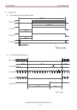
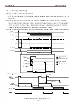
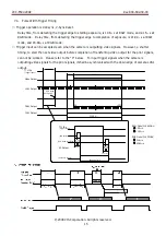
CIS VISION:elite VCC-F60U29GE, Operational Manual
The CIS VISION:elite VCC-F60U29GE offers cutting-edge technology in a compact design. Enhance your security with advanced features and high-quality imaging. Ensure optimal performance by following the Operational Manual available for free download on our website. Experience peace of mind with this top-of-the-line surveillance product.
Share
Download


Reviews:
No comments
Related manuals for VISION:elite VCC-F60U29GE

Holo360
Brand: Acer Pages: 18

T8
Brand: VEKOOTO Pages: 18
M2
Brand: laxihub Pages: 82

C3
Brand: UMAX Technologies Pages: 20

F-1
Brand: Canon Pages: 4
DIGITAL IXUS 430
Brand: Canon Pages: 2
EOS C100
Brand: Canon Pages: 6

3235B001
Brand: Canon Pages: 28
EOS C300 Mark II
Brand: Canon Pages: 16
Speedlite 277T
Brand: Canon Pages: 19
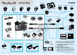
PowerShot G6
Brand: Canon Pages: 2
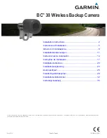
BC
Brand: Garmin Pages: 19

Digital Elph SD500
Brand: Canon Pages: 6

Canonet G III QL17
Brand: Canon Pages: 14
80D Experience
Brand: Canon Pages: 15
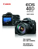
40D - EOS 40D DSLR
Brand: Canon Pages: 44
Digial IXUS 330
Brand: Canon Pages: 123
CANON EOS 1100D
Brand: Canon Pages: 112


