PN-2955H-A
- 12 -
051-3396-90
NJM2386ADL3-33-TE1
Positive Voltage Regulator 3.3V
051-3516-90
S-1132B33-U5T1G
Positive Voltage Regurator 3.3V
051-3517-90
impossible of exchange (LT3481EMSE#TRPBF)
Step-Down Switching Regulator
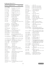
Terminal Description
BD (Pin 1):
This pin connects to the anode of the boost Schottky diode.
BOOST (Pin 2):
This pin is used to provide a drive voltage, higher than the input
voltage, to the internal bipolar NPN power switch.
SW (Pin 3):
The SW pin is the output of the internal power switch. Connect this
pin to the inductor, catch diode and boost capacitor.
VIN (Pin 4):
The VIN pin supplies current to the LT3481's internal regulator and
to the internal power switch. This pin must be locally bypassed.
RUN/SS (Pin 5):
The RUN/SS pin is used to put the LT3481 in shutdown mode. Tie
to ground to shut down the LT3481. Tie to 2.3V or more for nor-
mal operation. If the shutdown feature is not used, tie this pin to
the VIN pin.
PG (Pin 6):
The PG pin is the open collector output of an internal comparator.
PG remains low until the FB pin is within 10% of the final regula-
tion voltage. PG output is valid when VIN is above 3.5V and RUN/
SS is high.
BIAS (Pin 7):
The BIAS pin supplies the current to the LT3481's internal regula-
tor. Tie this pin to the lowest available voltage source above 3V
(typically VOUT). This architecture increases efficiency especially
when the input voltage is much higher than the output.
FB (Pin 8):
The LT3481 regulates the FB pin to 1.265V. Connect the feedback
resistor divider tap to this pin.
VC (Pin 9):
The VC pin is the output of the internal error amplifier. The volt-
age on this pin controls the peak switch current. Tie an RC net-
work from this pin to ground to compensate the control loop.
RT (Pin 10):
Oscillator Resistor Input. Connecting a resistor to ground from this
pin sets the switching frequency.
Exposed Pad (Pin 11):
Ground. The Exposed Pad must be soldered to PCB.
051-5417-38
R3112N271A-TR-FA
Precision Vlotage Down Detector 2.7V
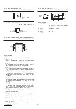
Terminal description
pin
1: OUTPUT
: N channel open drain output.
This terminal will output L, if the voltage of
VDD becomes lower than the setting voltage.
pin
2: VDD
: Positive supply voltage.
pin
3: GND
: Ground.
pin
4: N.C.
: Not in use.
pin
5: CD
: Delay time capacitor.
5
4
3
2
1
Ground
N.C.
Power Outut
Control in, H = ON.
VCC
3
1
2
3
5
4
Vin
Ground
Control (H= On)
Vout
Ground
No Connectin
RT
V C
F B
B I A S
P G
10
9
8
7
6
B D
B O O S T
S W
V I N
R U N / S S
1
2
3
4
5
TO P V I E W
11
1
2
3
5
4
CD
N.C.
OUTPUT
VDD
GND
+
-
Vref
OUTPUT
1
GND
3
VDD
2
CD
5
N.C.
4

