SWD/DEBUG
(1)
1
l
GND
2 R NRST
3 D SWDIO
4 C SWDCLK
SWD/DEBUG connector - Used for software development or flashing via SWD
Cannot be used when UART2 is enabled. Use an ST-Link debugger with OpenOCD or a J-Link debugger.
If for some reason you cannot flash using USB DFU or UART1 you can reinstall firmware using this port.
BUZZER
(12)
1
n
BUZZER- (B-)
2
l
(B+) / 5v
BUZZER
Use 5V and BUZZER- to connect to an external buzzer.
5.0v
is also supplied when powering via USB.
NOTE:
You can check the transponder LED is working by using a mobile phone camera pointed straight at the LED when the transponder is enabled via the
board and in the software. The LED will pulse an infrared signal which usually shows up purple via a mobile phone camera.
UART4 socket
(1)
1
l
GND
2
5v
3
TXD/SWDCLK
4
RXD/ESC-TELEMETRY
UART4 connector - Used for
5.0v
Serial IO. (GPS, etc.)
TXD
MUST NOT
be used when SWD port is in use.
5.0v
is always supplied via the on-board voltage regulators, even when powering via USB.
RXD signal also available on the middle of the first 4 motor outputs when the ESC-TLM bridge is set to TLM.
I2C1 socket
(2)
1
l
GND
2
5v
3
SCL
4
SDA
I2C1 connector - Used for external sensors and OLED displays.
The
SCL
and
SDA
are
3.3v
signals.
5.0v
is also supplied when powering via USB.
IMPORTANT:
logic level converters are
REQUIRED
if your sensors use
5.0v
signals.
T2/TLM
(3)
1
t
T2
2
n
OUTPUT
3
u
TLM
T2/TLM select bridge pads
Create a solder bridge between
TWO PADS ONLY
to select the function of the OUTPUT pad.
a) bridge
t
and
n
to set the TLM pin to T2.
b) bridge
n
and
u
to set the TLM pin to TELEMETRY.
See ‘Receiver Connections’ section below.
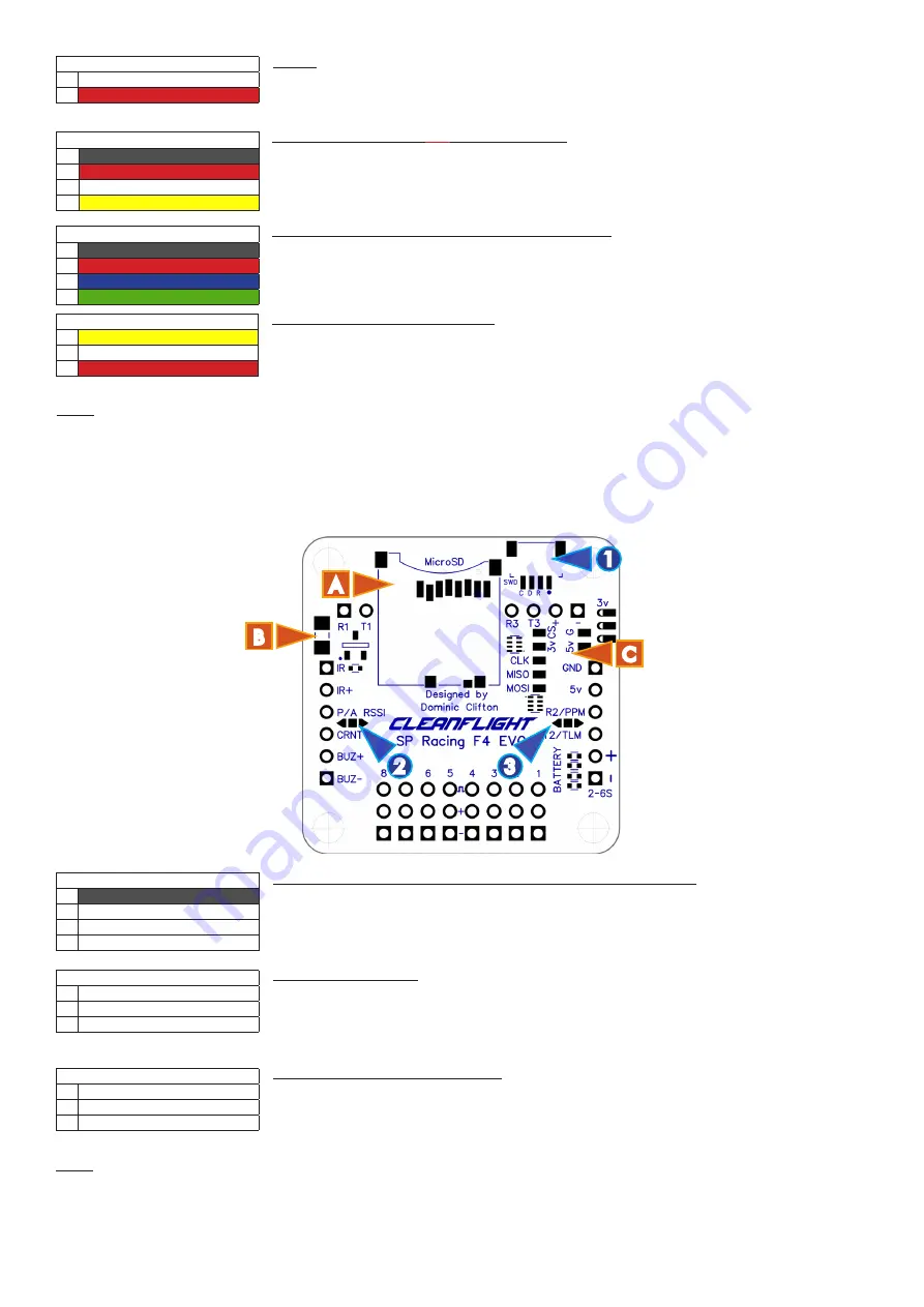
BOTTOM
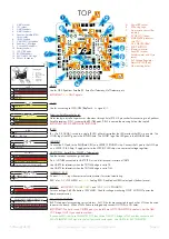
1. SWD debugging socket.
2. RSSI Analog/PWM bridge.
3. T2/TLM bridge.
A. MicroSD card socket
B. IR Transponder circuit.
C. SPI3/VTX pads.
2
1
SPRacingF4EVO
http://seriouslypro.com - http://cleanflight.com
Page 5
RSSI PWM / ANALOG SELECT
(3)
1
t
PWM RSSI
2
n
INPUT
3
u
ANAGLOG RSSI
RSSI PWM / ANALOG select bridge pads
Create a solder bridge between
TWO PADS ONLY
to select the function of the INPUT pad.
a) bridge
t
and
n
to use the “RSSI” pad for PWM RSSI - for
0 - 5v
PWM signals.
b) bridge
n
and
u
to use the “RSSI” pad for ANALOG RSSI - for
0 - 3.3v
Analog Signals.
NOTE:
When bridging select pads with solder, put a small blob of solder on two pads, let the solder cool, then bridge them together with a little more solder.
IMPORTANT: DO NOT CONNECT ALL THREE PADS TOGETHER.
A
3
C
B
TLM/VCC
(13)
1
p
ESC-TELEMETRY (UART4 RX)
2
n
OUTPUT
3
q
VIN
ESC-TELEMETRY/VCC select bridge pads
Create a solder bridge between
TWO PADS ONLY
to select the function of the OUTPUT pad.
a) bridge
p
and
n
to set the first 4 CENTER ESC pads to ESC-TELEMETRY (UART4)
b) bridge
n
and
q
to set the first 4 CENTER ESC pads to VCC/
VIN
.
See ‘Receiver Connections’ section below.


