background image

Disassembly

Removing the System Memory (RAM)  2  -  13

2.Disassembly

5.

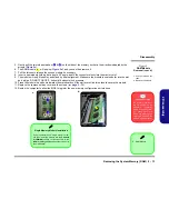
Gently pull the two release latches (

 & 

) on the sides of the memory socket in the direction indicated by the 

arrows (

Figure 9c

).


6.

The RAM module 

 will pop-up 

(

Figure 9d

)

, and you can then remove it

.

7.

Pull the latches to release the second module if necessary.

8.

Insert a new module holding it at about a 30° angle and fit the connectors firmly into the memory slot.

9.

The module will only fit one way as defined by its pin alignment. Make sure the module is seated as far into the slot 
as it will go. DO NOT FORCE IT; it should fit without much pressure.

10. Press the module in and down towards the mainboard until the slot levers click into place to secure the module.
11. Replace the component bay cover and the screws 

(see 

page 2 - 12

)

.

12. Restart the computer to allow the BIOS to register the new memory configuration as it starts up.

Figure 9

 RAM Module 

Removal (cont’d)

c. Pull the release lat-

ches.

d. Remove the module.

Contact Warning

Be careful not to touch 
the metal pins on the 
module’s connecting 
edge. Even the clean-
est hands have oils 
which can attract parti-
cles, and degrade the 
module’s performance.

7

8

9

c.

d.

7

8

9

Single Memory Module Installation

If your computer has a single memory mod-
ule, then insert the module into the 

Channel 

0 (JDIMM1) 

socket. In this case this is the 

lower memory socket

 (the socket closest to 

the mainboard).

9. RAM Module

Summary of Contents for W670SZQ

Page 1: ...W670SZQ ...

Page 2: ......

Page 3: ...Preface I Preface Notebook Computer W670SZQ Service Manual ...

Page 4: ...le or in part be reproduced translated transmitted or reduced to any machine readable form without prior consent from the vendor manufacturer or creators of this publica tion except for copies kept by the user for backup purposes Brand and product names mentioned in this publication may or may not be copyrights and or registered trademarks of their respective companies They are mentioned for ident...

Page 5: ...servicing and or upgrading components of the W670SZQ series notebook PC The following information is included Chapter 1 Introduction provides general information about the location of system elements and their specifications Chapter 2 Disassembly provides step by step instructions for disassembling parts and subsystems and how to upgrade elements of the system Appendix A Part Lists Appendix B Sche...

Page 6: ...eport a gas leak in the vicinity of the leak 4 Use only the power cord and batteries indicated in this manual Do not dispose of batteries in a fire They may explode Check with local codes for possible special disposal instructions 5 This product is intended to be supplied by a Listed Power Unit as follows AC Input of 100 240V 50 60Hz DC Output of 19 5V 6 15A 120 Watts minimum AC DC Adapter CAUTION...

Page 7: ... down properly and don t forget to save your work Remember to periodically save your data as data may be lost if the battery is depleted Do not expose the computer to any shock or vibration Do not place it on an unstable surface Do not place anything heavy on the computer Do not expose it to excessive heat or direct sunlight Do not leave it in a place where foreign matter or mois ture may affect t...

Page 8: ...rpose If you do not have access to a compatible outlet have a qualified electrician install one When you want to unplug the power cord be sure to disconnect it by the plug head not by its wire Make sure the socket and any extension cord s you use can support the total current load of all the connected devices Before cleaning the computer make sure it is disconnected from any external power supplie...

Page 9: ...ur hands or metal objects Battery Guidelines The following can also apply to any backup batteries you may have If you do not use the battery for an extended period then remove the battery from the computer for storage Before removing the battery for storage charge it to 60 70 Check stored batteries at least every 3 months and charge them to 60 70 Battery Disposal The product that you have purchase...

Page 10: ...nd mouse to their ports 5 Attach the AC DC adapter to the DC In jack on the left of the computer then plug the AC power cord into an outlet and connect the AC power cord to the AC DC adapter 6 Use one hand to raise the lid LCD to a comfortable viewing angle do not exceed 130 degrees use the other hand as illustrated in Figure 1 to support the base of the computer Note Never lift the computer by th...

Page 11: ... DVD Device 2 10 Removing the System Memory RAM 2 12 Removing and Installing a Processor 2 14 Removing the Fan Unit 2 17 Removing the Wireless LAN Module 2 18 Removing the MSATA Module 2 19 Removing the CCD 2 20 Part Lists A 1 Part List Illustration Location A 2 Top A 3 Bottom A 4 COMBO A 5 DVD DUAL A 6 HDD A 7 2nd HDD A 8 LCD A 9 Schematic Diagrams B 1 System Block Diagram B 2 Processor 1 7 DMI F...

Page 12: ...E IT8587 B 37 5VS 3VS 3 3VM 5VM B 38 1 05V B 39 VDD3 VDD5 B 40 1 5V or 1 35V 0 75VS 1 5VS B 41 POWER VCORE B 42 N14P NVVDD PEX FBVDDQ B 43 AC IN CHARGER B 44 AUDIO BOARD B 45 POWER SWITCH BOARD B 46 ODD to HDD BOARD B 47 Updating the FLASH ROM BIOS C 1 Download the BIOS C 1 Unzip the downloaded files to a bootable CD DVD or USB Flash drive C 1 Set the computer to boot from the external drive C 1 U...

Page 13: ...l is shipped with the computer Operating systems e g Windows 8 etc have their own manuals as do application softwares e g word processing and database programs If you have questions about those programs you should consult those manuals The W670SZQ series notebook is designed to be upgradeable See Disassembly on page 2 1 for a detailed description of the upgrade procedures for each specific compone...

Page 14: ...M 2 50GHz i3 4000M 2 40GHz 3MB L3 Cache 22nm DDR3L 1600MHz TDP 37W Core Logic Intel HM86 Chipset BIOS 48Mb SPI Flash ROM AMI BIOS Memory Two 204 Pin SO DIMM Sockets Supporting DDR3L 1600MHz Memory Memory Expandable up to 16GB The real memory operating frequency depends on the FSB of the processor Storage One Changeable 2 5 9 5mm 7mm h SATA HDD Factory Option One 12 7mm h Optical Device Type Drive ...

Page 15: ...luetooth 4 0 Factory Option Intel Wireless N 7260 Wireless LAN 802 11b g n Bluetooth 4 0 Factory Option Third Party Wireless LAN 802 11b g n Factory Option Third Party Wireless LAN 802 11a c Bluetooth 4 0 Factory Option Third Party Wireless LAN 802 11b g n Bluetooth 4 0 Card Reader Embedded Multi In 1 Card Reader MMC MultiMedia Card RS MMC SD Secure Digital Mini SD SDHC SDXC MS Memory Stick MS Pro...

Page 16: ...n Figure 1 Top View 1 PC Camera 2 Built In Microphone 3 PC Camera LED When the PC camera is in use the LED will be illuminated in red 4 LCD 5 Power Button 6 LED Indicator 7 Keyboard 8 Touchpad Buttons 5 3 4 6 1 2 7 8 Note that the Touchpad and Buttons valid operational area is that indicated within the red dotted lines 7 8 ...

Page 17: ...cator Front Right Side Views Figure 2 Front View 1 LED Indicator 2 Multi in 1 Card Reader Figure 3 Right Side View 1 Microphone In Jack 2 Headphone Out Jack 3 USB Ports 4 Optical Device Drive Bay 5 Emergency Eject Hole 6 Security Lock Slot FRONT VIEW 1 2 RIGHT SIDE VIEW 1 2 3 6 4 5 3 ...

Page 18: ...oduction External Locator Left Side Rear View Figure 4 Left Side View 1 DC In Jack 2 Vent 3 External Monitor Port 4 RJ 45 LAN Jack 5 Combined eSATA USB 3 0 Port 6 HDMI Out Port 7 USB 3 0 Ports LEFT SIDE VIEW 1 2 3 4 5 6 7 Figure 5 Rear View 1 Battery REAR VIEW 1 ...

Page 19: ...External Locator Bottom View Figure 6 Bottom View 1 Battery 2 Component Bay Cover 3 Vent 4 Multi in 1 Card Reader 5 Speakers Overheating To prevent your com puter from overhea ting make sure no thing blocks any vent while the computer is in use 2 3 1 4 3 5 5 3 3 ...

Page 20: ...Introduction 1 8 Mainboard Overview Top Key Parts 1 Introduction Mainboard Overview Top Key Parts Figure 7 Mainboard Top Key Parts 2 3 ...

Page 21: ... CPU Socket no CPU installed 3 Northbridge Platform Controller Hub 4 VGA Chip 5 KBC ITE IT8518 6 Mini Card Connector mSATA Module 7 Mini Card Connector WLAN Module 8 CMOS Battery Introduction Mainboard Overview Bottom Key Parts 1 9 1 Introduction Mainboard Overview Bottom Key Parts ...

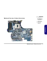
Page 22: ...Top Connectors Figure 9 Mainboard Top Connectors 1 External Monitor Port 2 RJ 45 LAN Jack 3 Combo eSATA USB Port 3 0 4 HDMI Out Port 5 USB Port 3 0 Connector 6 Speaker Cable Connector 7 Keyboard Cable Connector 8 Touchpad Cable Connector 9 Touchpad Cable Connector 10 11 9 7 8 6 5 1 2 3 4 ...

Page 23: ...ion Mainboard Overview Bottom Connectors 1 11 1 Introduction Mainboard Overview Bottom Connectors Figure 10 Mainboard Bottom Connectors 1 ODD Connector 2 HDD Connector 3 LCD Cable Connector 6 7 8 9 5 11 12 1 2 3 ...

Page 24: ...Introduction 1 12 1 Introduction ...

Page 25: ...embly process easier each section may have a box in the page margin Information contained under the figure will give a synopsis of the sequence of procedures involved in the disassembly procedure A box with a lists the relevant parts you will have after the disassembly process is complete Note The parts listed will be for the dis assembly procedure listed ONLY and not any previous disassembly step...

Page 26: ...c ing the connection make sure the connector is oriented in the same way The pin1 side is usually not indicated Pressure sockets for multi wire connectors To release this connector type grasp it at its head and gently rock it from side to side as you pull it out Do not pull on the wires themselves When replacing the connection do not try to force it The socket only fits one way Pressure sockets fo...

Page 27: ... pull on the wire 6 Peripherals Turn off and detach any peripherals 7 Beware of static discharge ICs such as the CPU and main support chips are vulnerable to static electricity Before handling any part in the computer discharge any static electricity inside the computer When handling a printed circuit board do not use gloves or other materials which allow static electricity buildup We suggest that...

Page 28: ...emove the HDD page 2 7 To remove the Optical Device 1 Remove the battery page 2 5 2 Remove the Optical device page 2 10 To remove the System Memory 1 Remove the battery page 2 5 2 Remove the system memory page 2 12 To remove and install a Processor 1 Remove the battery page 2 5 2 Remove the processor page 2 14 3 Install the processor page 2 16 To remove the Wireless LAN Module 1 Remove the battery...

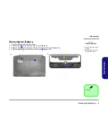
Page 29: ...ide the latch in the direction of the arrow Figure 1a 3 Slide the latch in the direction of the arrow and hold it in place Figure 1a 4 Slide the battery in the direction of the arrow Figure 1b 1 2 6 3 4 Figure 1 Battery Removal a Slide the latch and hold it in place b Slide the battery in the di rection of the arrow 1 a b 3 2 4 ...

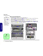
Page 30: ...ift the keyboard up being careful not to bend the keyboard ribbon cable Disconnect the keyboard ribbon cable from the locking collar socket and the keyboard LED cable from its locking collar Figure 2d 6 Carefully lift the keyboard off the computer Figure 2e 1 2 6 3 4 8 9 10 11 12 13 b d a 1 e 13 8 3 7 c 5 6 4 10 9 11 2 12 10 3 Center Cover Module 13 Keyboard 6 Screws Figure 2 Keyboard Removal a Re...

Page 31: ... s Manual when setting up a new hard disk Hard Disk Upgrade Process Figure 3 HDD Assembly Removal a Remove the screws Lift the component bay cov er off the computer 3 Component Bay Cover 2 Screws 1 Turn off the computer and remove the battery page 2 5 2 Locate the component bay cover and remove screws Figure 3a 3 Lift the component bay cover off the computer case by applying pressure at points if ...

Page 32: ...7 HDD System Warning New HDD s are blank Before you begin make sure You have backed up any data you want to keep from your old HDD You have all the CD ROMs and FDDs required to install your oper ating system and programs If you have access to the internet download the latest application and hardware driver updates for the op erating system you plan to install Copy these to a removable medi um 10 3...

Page 33: ...rives In some cases 7mm H hard disk drives will be installed For more information contact your distributor supplier and bear in mind your warranty terms Figure 5 Foam Rubber Insert for 7mm H HDDs If you are replacing a 9 5mm H HDD with a 7mm H HDD then insert the foam rubber insert as shown above If you are replacing a 7mm H HDD with a 9 5mm H HDD then remove the foam rubber insert ...

Page 34: ...ms using a finger to do this then use a non abrasive non sharp object e g a coin to lift the cover up before removal 4 Remove the screw at point Figure 6b 5 Use a screwdriver to carefully push out the optical device at point Figure 6c 1 2 3 4 5 6 8 7 3 Component Bay Cov er 8 Optical Device 3 Screws 1 3 a 2 4 b 6 8 c 7 5 Figure 6 Optical Device Removal a Remove the screws Lift the component bay cov...

Page 35: ...w holes should line up 10 Reinsert the component bay cover by placing it on the bottom case assembly and aligning the pins at the bottom of the cover with the slots in the case to ensure a proper fit Press down on the cover to make sure it fits tightly 11 Replace the screws and battery 12 Restart the computer to allow it to automatically detect the new device 10 9 10 10 11 10 Bezel g h 10 e f 9 10...

Page 36: ...DIMM supporting DDR3L Up to 1600 MHz The main memory can be expanded up to 16GB The SO DIMM modules supported are 1024MB and 2048MB DDRIII Modules The total memory size is automatically detected by the POST routine once you turn on your computer Memory Upgrade Process 3 Component Bay Cov er 2 Screws 1 Turn off the computer turn it over and remove the battery page 2 5 2 Remove screws from the compo...

Page 37: ...sure 10 Press the module in and down towards the mainboard until the slot levers click into place to secure the module 11 Replace the component bay cover and the screws see page 2 12 12 Restart the computer to allow the BIOS to register the new memory configuration as it starts up Figure 9 RAM Module Removal cont d c Pull the release lat ches d Remove the module Contact Warning Be careful not to t...

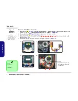
Page 38: ...page 2 7 2 The CPU heat sink will be visible at point Figure 10a 3 Loosen the CPU heat sink screws in the order the reverse order as indicated on the label Figure 10b 4 Carefully it may be hot remove the heat sink unit off the computer Figure 10c A 8 7 6 5 4 3 2 1 B a b 4 1 7 A B c 6 3 2 5 8 B Heat Sink 8 Screws Figure 10 Processor Removal a Locate the CPU heat sink b Remove the screws c Carefully...

Page 39: ... the process to install a new CPU 8 When re inserting the CPU pay careful attention to the pin alignment it will fit only one way DO NOT FORCE IT C D d D C e C Caution The heat sink and CPU area in general contains parts which are subject to high temperatures Allow the area time to cool before remov ing these parts D CPU Figure 11 Processor Removal cont d d Turn the release latch to unlock the CPU...

Page 40: ...f it is a new unit 3 Insert the heat sink as indicated in Figure 12c 4 Tighten the CPU heat sink screws in the order the order as indicated on the label and Figure 12d 5 Replace the CPU fan component bay cover and tighten the screws page 2 14 A B C D 1 2 3 4 5 6 7 8 4 1 7 6 3 2 5 8 b B a D Note Tighten the screws in the order as indicated on the label A c d C D C Figure 12 Processor Installation a...

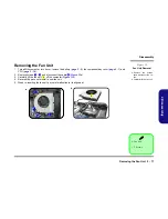
Page 41: ...age 2 14 2 Remove screws and disconnect the cable Figure 13a 3 Carefully lift the fan unit off the computer Figure 13c 4 Reverse the process to install a new fan unit 5 When re inserting the fan unit pay careful attention to its alignment 1 3 4 5 a b 5 2 3 1 4 5 Fan Unit 3 Screws Figure 13 Fan Unit Removal a Remove the screws ansd disconnect the ca ble b Carefully lift the fan unit ...

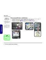
Page 42: ...on the mainboard Figure 14a 3 Carefully disconnect the cables and then remove the screw Figure 14b 4 The Wireless LAN module Figure 14c will pop up and you can remove it from the computer 1 2 3 4 5 b c a 2 3 5 1 5 4 5 Wireless LAN Module 1 Screw Figure 14 Wireless LAN Module Removal a Locate the WLAN b Disconnect the cables and remove the screw c The WLAN module will pop up Note Make sure you reco...

Page 43: ... cover page 2 7 2 Locate the module it is visible at point Figure 15a 3 Carefully remove the screw from the module Figure 15b 4 Lift the module up and off the computer Figure 15c Figure 15 MSATA Module Removal a Locate the module b Remove the screw c The module will pop up d Lift the module up off the socket 1 2 3 a b 1 3 2 3 c d 3 MSATA Module 1 Screw ...

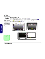
Page 44: ... top case up forming a 90 degree angle Push the LCD front cover upwards before carefully lifting it up 4 Remove the LCD front cover Figure 16c 1 4 5 5 c b a 1 5 5 3 2 4 5 LCD Front Cover Figure 16 CCD Removal a Run your fingers around the inner frame of the LCD panel at the points indicated by the arrows b Lay the computer down on a flat surface with the top case up forming a 90 degree angle Push ...

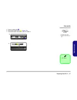
Page 45: ... 2 21 2 Disassembly 5 Disconnect the cable 6 Remove the CCD module Figure 17f 7 Reverse the process to install a new CCD module 6 7 e d 7 6 7 CCD Module Figure 17 CCD Removal cont d d Disconnect the cable e Remove the CCD mod ule ...

Page 46: ...Disassembly 2 22 2 Disassembly ...

Page 47: ... Your organization may use a different system so be sure to cross check any relevant documentation Note Some assemblies may have parts in common especially screws However the part lists DO NOT indicate the total number of duplicated parts used Note Be sure to check any update notices The parts shown in these illustrations are appropriate for the system at the time of publication Over the product l...

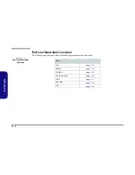
Page 48: ...tion The following table indicates where to find the appropriate part list illustration Table A 1 Part List Illustration Location Part Top page A 3 Bottom page A 4 COMBO page A 5 DVD Dual Drive page A 6 HDD page A 7 2nd HDD page A 8 LCD page A 9 ...

Page 49: ...Top A 3 A Part Lists Top Figure A 1 Top ...

Page 50: ...A 4 Bottom A Part Lists Bottom Figure A 2 Bottom ...

Page 51: ...COMBO A 5 A Part Lists COMBO 非耐落 Figure A 3 COMBO ...

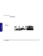
Page 52: ...A 6 DVD DUAL A Part Lists DVD DUAL Figure A 4 DVD DUAL 非耐落 ...

Page 53: ...HDD A 7 A Part Lists HDD Figure A 5 HDD ...

Page 54: ...A 8 2nd HDD A Part Lists 2nd HDD Figure A 6 2nd HDD ...

Page 55: ...LCD A 9 A Part Lists LCD Figure A 7 LCD ...

Page 56: ...A 10 A Part Lists ...

Page 57: ...age B 39 Processor 6 7 GND Page B 8 Lynx 4 9 Page B 24 VDD3 VDD5 Page B 40 Processor 7 7 RSVD Page B 9 Lynx 5 9 Page B 25 1 5V or 1 35V 0 75VS 1 5VS Page B 41 DDR3 SO DIMM_1 Page B 10 Lynx 6 9 Page B 26 POWER VCORE Page B 42 DDR3 SO DIMM_2 Page B 11 Lynx 7 9 Page B 27 N14P NVVDD PEX FBVDDQ Page B 43 PS8625 Page B 12 Lynx 8 9 Page B 28 AC IN CHARGER Page B 44 PANEL INVERTER Page B 13 Lynx 9 9 Page ...

Page 58: ...thout ASM1464 W650 BOM 6 77 W6508 D05 W6X0 PCB 6 71 W6508 D05 15 750M N14P GT 35W 40W 740M N14P GS 25W 30W 5V 3V 5VS 3VS USB2 0 908 Balls Nvidia Fermi N14P GT RAM SIZE2GB 128X64M DDR3 VDD3 VDD5 DMI 4 USB2 0 PORT0 rPGA946B 37 5x37 5mm 5 Gbps USB3 0 32 768 KHz REALTEK SATA I II III 6 0Gb s 1067 1333 1600 MHz DDR3 1 35 CCD Mic USB11 VIA1802S 33 MHz THERMAL SENSOR 100 MHz 14 14 1 6mm PROCESSOR SMART F...

Page 59: ...17 DMI_TXN_0 D18 DMI_RXP_3 A20 DMI_RXP_2 B20 DMI_RXP_1 C20 DMI_RXP_0 D20 DMI_RXN_3 A21 DMI_RXN_2 B21 DMI_RXN_1 C21 DMI_RXN_0 D21 8 30 PCBA qªý 1R 0_04 2R 0_04 4R 0_04 3R 0_04 5R 0_04 6R 0_04 W40SR PCBA W650SR PCBA VCCIOA_OUT 5 6 PEG_IRCOMP Haswell rPGA Processor 1 7 DMI PEG FDI 1 2 4mils 8mils 20120201 H7 H8_0D4_4 H8 H8_0D4_4 H5 H8_0D4_4 C559 0 1u_10V_X7R_04 C539 0 22u_10V_X5R_04 C546 0 22u_10V_X5...

Page 60: ... SM_DRAMRST AN3 PRDY AR29 PREQ AT29 TCK AM34 TMS AN33 TRST AM33 TDI AM31 TDO AL33 DBR AP33 BPM_N_0 AR30 BPM_N_1 AN31 BPM_N_2 AN29 BPM_N_3 AP31 BPM_N_4 AP30 BPM_N_5 AN28 BPM_N_6 AP29 BPM_N_7 AP28 PWRGOOD AL34 PM_SYNC AT28 FC AK31 R52 3 32K_1 _04 R386 100_1 _04 R376 2K_1 _04 R387 100_1 _04 PCH_SSC_N PCH_SSC_P H_THRMTRIP_R_N R58 200_04 SSC CLOCK TERMINATION STUFF R4R15 R4R12 ONLY WHEN SSC CLOCK NOT U...

Page 61: ..._41 J8 SB_DQ_40 G7 SB_DQ_39 M5 SB_DQ_38 L5 SB_DQ_35 M4 SB_DQ_33 M2 SB_DQ_29 AN1 SB_DQ_28 AM1 SB_DQ_27 AJ2 SB_DQ_26 AJ1 SB_DQ_25 AK4 SB_DQ_24 AJ4 SB_DQ_23 AN6 SB_DQ_22 AN5 SB_DQ_21 AT6 SB_DQ_20 AT5 SB_DQ_19 AM6 SB_DQ_18 AM5 SB_DQ_17 AR6 SB_DQ_16 AR5 SB_DQ_15 AN11 SB_DQ_14 AM12 SB_DQ_13 AR11 SB_DQ_12 AT11 SB_DQ_11 AM11 SB_DQ_10 AN12 SB_DQ_9 AR12 SB_DQ_8 AT12 SB_DQ_7 AN18 SB_DQ_6 AN17 SB_DQ_5 AT17 SB...

Page 62: ...C AF35 VCC AF34 VCC AF33 VCC AF32 VCC AF31 VCC AF30 VCC AF29 VCC AF28 VCC AF27 VCC AF26 VCC AF25 VCC AE34 VCC AG34 VCC AG28 VCC AE30 VCC AE28 VCC AE32 VCC AE26 VCC AD35 VCC AD33 VCC AD32 VCC AD30 VCC AD29 VCC AD27 VCC AD26 VCC AD34 VCC AC34 VCC AD31 VCC AC32 VCC AD28 VCC AC30 VCC AD25 VCC AC28 VCC AB35 VCC AC26 VCC AB32 VCC AB34 VCC AB33 VCC AB31 VCC AB30 VCC AB28 VCC AB27 VCC AB25 VCC AB29 VCC AB...

Page 63: ...MP E24 EDP_TXP_1 P34 EDP_TXP_0 R35 EDP_TXN_1 N34 EDP_TXN_0 P35 EDP_HPD P27 EDP_AUXP N27 EDP_AUXN M27 DDID_TXDP_3 P30 DDID_TXDN_3 N30 DDID_TXDP_2 R31 DDID_TXDN_2 P31 DDID_TXDP_1 P28 DDID_TXDN_1 N28 DDID_TXDP_0 R29 DDID_TXDN_0 P29 DDIC_TXCP_3 V33 DDIC_TXCP_1 V35 DDIC_TXCN_1 U35 DDIC_TXCP_0 U34 DDIC_TXCN_0 T34 DDIB_TXBP_3 V31 DDIB_TXBP_0 U28 DDIB_TXBN_0 T28 DDIC_TXCN_2 U32 DDIC_TXCP_2 T32 DDIC_TXCN_3...

Page 64: ...AA31 VSS AA27 VSS AA25 VSS AA11 VSS A7 VSS A4 VSS A33 VSS A31 VSS A3 VSS A29 VSS A27 VSS A25 VSS A22 VSS A19 VSS A16 VSS A13 VSS A10 VSS AP13 VSS AC31 VSS AB9 VSS W25 VSS AP7 VSS AE3 VSS AE29 VSS AE25 VSS AR10 Haswell rPGA EDS 7 OF 9 U26G RSVD AK33 VSS_SENSE AK35 VSS W9 VSS W4 VSS W35 VSS W3 VSS W10 VSS W1 VSS V34 VSS V32 VSS V30 VSS V28 VSS V11 VSS U27 VSS U11 VSS T9 VSS T7 VSS T6 VSS T4 VSS T35 ...

Page 65: ...cessor 7 7 RESERVED CFG3 CFG5 CFG4 CFG2 CFG6 CFG7 R359 49 9_1 _04 R357 49 9_1 _04 R384 49 9_1 _04 Default NOTE PHYSICAL_DEBUG_ENABLED DFX PRIVACY 0 ENABLED SET DFX ENABLED BIT IN DEBUG INTERFACE MSR 1 DISABLED Default CFG3 DEFENSIVE PULL DOWN SITE CFG5 CFG4 CFG2 CFG2 CFG6 CFG 6 5 PCI EXPRESS STATIC LANE REVERSAL FOR ALL PEG PORTS 1 DEFAULT NORMAL OPERATION LANE DEFINITION MATCHES 0 LANE REVERSAL P...

Page 66: ...49 165 DQ50 175 DQ51 177 DQ52 164 DQ53 166 DQ54 174 DQ55 176 DQ56 181 DQ57 183 DQ58 191 DQ59 193 DQ60 180 DQ61 182 DQ62 192 DQ63 194 BA0 109 BA1 108 RAS 110 WE 113 CAS 115 S0 114 S1 121 CKE0 73 CKE1 74 CK0 101 CK0 103 CK1 102 CK1 104 SDA 200 SCL 202 SA1 201 SA0 197 DM0 11 DM1 28 DM2 46 DM3 63 DM4 136 DM5 153 DM6 170 DM7 187 DQS0 12 DQS1 29 DQS2 47 DQS3 64 DQS4 137 DQS5 154 DQS6 171 DQS7 188 DQS0 1...

Page 67: ...Q49 165 DQ50 175 DQ51 177 DQ52 164 DQ53 166 DQ54 174 DQ55 176 DQ56 181 DQ57 183 DQ58 191 DQ59 193 DQ60 180 DQ61 182 DQ62 192 DQ63 194 BA0 109 BA1 108 RAS 110 WE 113 CAS 115 S0 114 S1 121 CKE0 73 CKE1 74 CK0 101 CK0 103 CK1 102 CK1 104 SDA 200 SCL 202 SA1 201 SA0 197 DM0 11 DM1 28 DM2 46 DM3 63 DM4 136 DM5 153 DM6 170 DM7 187 DQS0 12 DQS1 29 DQS2 47 DQS3 64 DQS4 137 DQS5 154 DQS6 171 DQS7 188 DQS0 ...

Page 68: ...B ground plane with thedeviceGND pins of the PS8625 connected to separate GND island GNDA for the device The GND island GNDA should be connected to themain GND plane GND with a single point connection by useof a widePCB trace 4 Place the4 7uF decoupling Capacitor C4 for VDDIOX close to VDDIOX pin 5 The GND of the4 7uF capacitor C4 for VDDIOX should beplaced close to theGND of 4 7uF capacitor C5 be...

Page 69: ...6R 5 3 4 S D G Q31A MTDN7002ZHS6R 2 6 1 C366 0 1u_50V_Y5V_06 VDDIO RLV_LNK LVDS single link or dual link selection internal pull down 80K L Single link LVDS H Dual link LVDS RLV_LNK GPIO0 11 R7 4 7K_04 3 3VS PANEL_VCC_EN 11 R348 0_04 VDDIO 11 R354 100K_04 U24B 74LVC08PW 4 5 6 14 7 PJ15 OPEN_2A 1 2 U24C 74LVC08PW 9 10 8 14 7 R12 4 7K_04 J_LCD2 50238 0407N 001 1 3 5 7 9 11 13 15 17 19 21 23 25 27 29...

Page 70: ...0 22u_10V_X5R_04 VGA_STRAP1 C172 0 22u_10V_X5R_04 M_STRAP_REF0 C152 0 1u_16V_Y5V_04 C190 0 1u_10V_X7R_04 C162 0 22u_10V_X5R_04 C267 4 7u_6 3V_X5R_06 R408 40 2K_1 _04 C236 0 22u_10V_X5R_04 C331 4 7u_6 3V_X5R_06 C625 22u_6 3V_X5R_08 C269 0 22u_10V_X5R_04 C588 18p_50V_NPO_04 C158 0 22u_10V_X5R_04 C208 0 22u_10V_X5R_04 X_OUTBUFF FCM1005KF 600T03 6 19 31001 238 VID_PLLVDD C254 1u_6 3V_X5R_04 C281 0 22u...

Page 71: ...21 FBB_D39 G21 FBB_D38 E21 FBB_D37 D21 FBB_D36 G24 FBB_D35 E24 FBB_D34 G23 FBB_D33 F24 FBB_D32 B8 FBB_D31 C8 FBB_D30 A8 FBB_D29 D8 FBB_D28 B11 FBB_D27 D11 FBB_D26 C11 FBB_D25 A11 FBB_D24 C5 FBB_D23 B5 FBB_D22 C4 FBB_D21 B3 FBB_D20 C1 FBB_D19 D3 FBB_D18 D4 FBB_D17 C2 FBB_D16 F3 FBB_D15 E2 FBB_D14 G4 FBB_D13 F4 FBB_D12 F6 FBB_D11 E6 FBB_D10 F5 FBB_D9 G6 FBB_D8 G12 FBB_D7 F12 FBB_D6 G11 FBB_D5 F11 FB...

Page 72: ...A8 T8 A9 R3 A10 L7 A11 R7 BA0 M2 BA1 N8 NC4 L9 CKE K9 CK J7 CK K7 NC1 J1 NC2 J9 ODT K1 VDD B2 VDD D9 VDD G7 VDD K2 VDD K8 VDD N1 VDD N9 VDD R1 VDD R9 VDDQ A1 VDDQ C1 VDDQ C9 VDDQ D2 VDDQ E9 VDDQ F1 VSS M1 VSS M9 VSS P1 VSS P9 VSS T1 VSS T9 VSSQ B1 VSSQ B9 VSSQ D1 VSSQ D8 VREFDQ H1 VSS A9 VSS B3 VSS E1 VSS J2 VSS J8 VREFCA M8 A12 N7 A13 T3 NC3 L1 A14 NC6 T7 DQL0 E3 DQL1 F7 DQL2 F2 DQL3 F8 DQL4 H3 D...

Page 73: ..._1 _04 C860 1u_6 3V_X5R_04 C356 0 1u_10V_X7R_04 C854 1u_6 3V_X5R_04 R553 243_1 _04 C858 1u_6 3V_X5R_04 U15 K4W2G1646E BC11 RAS J3 CAS K3 WE L3 CS L2 A0 N3 A1 P7 A2 P3 A3 N2 A4 P8 A5 P2 A6 R8 A7 R2 A8 T8 A9 R3 A10 L7 A11 R7 BA0 M2 BA1 N8 NC4 L9 CKE K9 CK J7 CK K7 NC1 J1 NC2 J9 ODT K1 VDD B2 VDD D9 VDD G7 VDD K2 VDD K8 VDD N1 VDD N9 VDD R1 VDD R9 VDDQ A1 VDDQ C1 VDDQ C9 VDDQ D2 VDDQ E9 VDDQ F1 VSS M...

Page 74: ...O16 GK208 GF117 COMMON BGA_0908_P080_P085_P100_290X290 U33Q N14P GT QS AN11 JTAG_TRST AP12 JTAG_TDO AM11 JTAG_TDI AP11 JTAG_TMS AM10 JTAG_TCK K3 THERMDP K4 THERMDN P1 GPIO21 P4 GPIO20 R8 GPIO16 M4 GPIO13 N3 GPIO12 M5 GPIO11 L1 GPIO10 M2 GPIO9 M1 GPIO8 N8 GPIO7 M7 GPIO6 L7 GPIO5 P7 GPIO4 P5 GPIO3 L6 GPIO2 M3 GPIO1 P6 GPIO0 R6 I2CB_SDA R7 I2CB_SCL R3 I2CC_SDA R2 I2CC_SCL T3 I2CS_SDA T4 I2CS_SCL 8 17...

Page 75: ... ND W20 G ND W18 G ND W17 G ND W15 G ND W13 G ND V23 G ND V21 G ND V19 G ND V16 G ND V14 G ND V12 G ND U23 G ND U21 G ND U19 G ND U16 G ND U14 G ND U12 G ND T7 G ND T5 G ND T32 G ND T28 G ND 13 17 NVVDD COMMON BGA_0908_P080_P085_P100_290X290 U3 3H N14P GT QS Y22 V DD Y20 V DD Y18 V DD Y17 V DD Y15 V DD Y13 V DD W23 V DD W21 V DD W19 V DD W16 V DD W14 V DD W12 V DD V22 V DD V20 V DD V18 V DD V17 V ...

Page 76: ...6 7 8 R73 150_1 _04 R96 33_04 L5 0_04 C139 10p_50V_NPO_04 C138 22p_50V_NPO_04 C124 22p_50V_NPO_04 C581 0 22u_10V_X5R_04 C123 10p_50V_NPO_04 C151 10p_50V_NPO_04 5VS 3 3VS 5VS 3 3VS DAC_DDCADATA 23 DAC_HSYNC 23 DAC_VSYNC 23 DAC_GREEN 23 DAC_BLUE 23 DAC_DDCACLK 23 DAC_RED 23 FGRN HSYNC DDCLK FRED FBLUE CRT VSYNC DDCDATA HSYNC VSYNC_C DDCDATA FGRN HSYNC_C VSYNC FRED FBLUE DDCLK H27 H7_0D2_8 GND 5VS 12...

Page 77: ... VIN 4 VIN 5 EN 3 VOUT 1 GND 2 W650SR INTVRMEN Integrated SUS 1 05V VRM Enable High Enable Internal VRs Low Enable External VRs PCH_INTVRMEN NO REBOOT STRAP NO REBOOT STRAP HDA_SPKR High Enable HDA_SPKR R318 1K_04 3 3VS Closed to U4 Layout Note R505 1K_04 3 3VS HDADOCKEN_N R517 10K_04 INTVRMEN INTEGRATED SUS 1 05V VRM ENABLE HIGH ENABLE INTERNAL VR S LOW ENABLE EXTERNAL VR S ODD Zero Power ODD C58...

Page 78: ...L_CLK1 29 LPC_AD1 30 36 LPC_AD0 30 36 SML1CLK 36 SML1DATA 36 SERIRQ 30 36 LPC_FRAME 30 36 LPC_AD3 30 36 LPC_AD2 30 36 R152 0_04 R160 0_04 SMD_VGA_THERM 17 36 SMC_VGA_THERM 17 36 VDD3 17 20 22 24 27 28 29 30 32 33 36 37 38 39 40 43 R179 10K_04 SPI_WP _1 SPI_HOLD _1 R153 2 2K_04 PCH_SPI_DQ3 HSPI_MSO 36 R151 2 2K_04 HSPI_MSI 36 SPI_SI_R SPI_SO_R R163 10K_04 R115 10K_04 SPI_WP _0 SPI_HOLD _0 SERIRQ VD...

Page 79: ...T R427 PCIE_WAKE SUS_CK VDD3 3 3VS RTCVCC R112 8 2K_04 R180 8 2K_04 PM_BATLOW Disabled RN3 10K_8P4R_04 1 2 3 4 5 6 7 8 PM_SLP_LAN R183 10K_04 R178 100K_04 R491 1K_04 R166 10K_04 R510 330K_04 Enabled DEFAULT ALL_SYS_PWRGD DSWODVREN PM_CLKRUN PM_MPWROK PM_PCH_PWROK_R SUSWARN SY S_RESET T20 R148 0_04 VDD3 VDD3 VDD3 SWI SUSWARN Lynx Point M DMI FDI PWRGD VDD3 AC_PRESENT PWR_BTN RSMRST R489 10K_04 LPT_...

Page 80: ...PCI 1 1 SPI Boot BIOS Strap R508 0_04 R181 1M_04 3 3VS DAC_GREEN 19 3 3VS 3 6 9 10 11 12 19 20 21 22 24 26 27 28 29 30 31 32 33 34 35 36 37 41 5VS 12 19 20 30 33 34 35 37 41 42 DAC_VSYNC 19 DAC_HSYNC 19 DAC_BLUE 19 DAC_RED 19 BLON 12 NB_ENAVDD 12 36 DAC_DDCADATA 19 DAC_DDCACLK 19 dGPU_PWR_EN 36 42 SATA_ODD_DA 20 24 PLT_RST 3 23 30 PME 32 36 DPC_HPD 34 dGPU_RST 36 PERSTB 13 PLT_RST 3 23 30 L_BRIGHT...

Page 81: ...ATA_ODD_PRSNT VDD3 SATA_DET 4 DGPU_SELECT SCI DGPU_SELECT 23 GFX_CRB_DET R439 0_04 SV_DET C591 0 1u_10V_X5R_04 R123 0_04 SV DETECT DEFAULT H_CPUPWRGD 3 3VS 3 3VS 3 3VS 3 3VS 3 3VS 3 6 9 10 11 12 19 20 21 22 23 26 27 28 29 30 31 32 33 34 35 36 37 41 3 3VS GFX_CRB_DET SATA_ODD_PRSNT 20 SCI 36 3 3V 2 3 12 17 20 25 27 28 29 31 33 35 37 38 40 42 H_PECI 3 36 GA20 36 SMI 36 CPU_RST_N 3 H_THRMTRIP_R_N 3 K...

Page 82: ...ne 4 GLAN CARD READER Lane 5 X Lane 6 X Lane 7 X Lane 8 X USB_PN10 29 Usage USB_PN0 31 USB_PP1 30 USB_PN1 30 USB_PP10 29 USB_PP0 31 1 5VS 20 22 26 27 28 40 42 USB_PP11 30 USB_PN11 30 LPT_PCH_M_EDS USB PCIe 9 OF 11 U32I USB3TP6 BE28 USB3TN6 BD27 USB3RP6 AP29 USB3RN6 AR29 USB3TP5 BC26 USB3TN5 BE26 USB3RP5 AV29 USB3RN5 AW29 PETP1 USB3TP3 BC32 PERP2 USB3RP4 AR31 PETP2 USB3TP4 BB33 USB3TP2 BC24 PETN2 U...

Page 83: ... 38 39 40 43 1 05V_LAN_M 3 3VS 1 05V_LAN_M 3 3VS 3 3V_PCH 1 5VS 1 5VS VCCA_DAC_1_2 1 5VS 1 05VM 1 05V_LAN_M 1 05V_LAN_M 1 5VS 20 22 25 27 28 40 42 1 05V_LAN_M 3 5 27 38 41 42 3 3V 2 3 12 17 20 24 25 27 28 29 31 33 35 37 38 40 42 3 3VS 3 6 9 10 11 12 19 20 21 22 23 24 27 28 29 30 31 32 33 34 35 36 37 41 C326 0 1u_10V_X5R_04 VCCA_DAC1 5V CO LAY C304 22u_6 3V_X5R_08 C615 100u_6 3V_B_A C289 22u_6 3V_X...

Page 84: ...S_VCC_ASEPCI L15 HCB1608KF 121T25 L29 HCB1608KF 121T25 L16 HCB1608KF 121T25 L12 HCB1608KF 121T25 L28 HCB1608KF 121T25 L30 HCB1608KF 121T25 L20 HCB1608KF 121T25 L17 HCB1005KF 121T20 L22 HCB1608KF 121T25 L23 HCB1005KF 121T20 3 3VS DCPSUS2 1 05V_LAN_M 1 05V_LAN_M 3 3V_PCH 1 05V_LAN_M 1 05V_LAN_M 3 3VS 3 3VS 3 3VS 1 05V_LAN_M 3 3VS 1 05V_LAN_M 1 05V_LAN_M 1 05V_LAN_M 3 3VS RTCVCC 3 3VA_1 5A_HDA_IO 3 3...

Page 85: ...0 VSS AD18 VSS BB42 VSS BC22 VSS BC28 VSS AD6 VSS AD40 LPT_PCH_M_EDS 10 OF 11 U32J VSS AV31 VSS BB25 VSS AV40 VSS AV33 VSS AV13 VSS D42 VSS AT36 VSS AT26 VSS AT20 VSS AT17 VSS AT29 VSS AV24 VSS N12 VSS N39 VSS N35 VSS N6 VSS P24 VSS P22 VSS P30 VSS P28 VSS P26 VSS P32 VSS R12 VSS R2 VSS R16 VSS R14 VSS R38 VSS R34 VSS R44 VSS T43 VSS R8 VSS U16 VSS U10 VSS U28 VSS U34 VSS U38 VSS U6 VSS U42 VSS V1...

Page 86: ... PCIE_TXN3_WLAN 25 WLAN_DET 36 CL_RST 1 21 BUF_PLT_RST 23 32 33 36 PCIE_RXP3_WLAN 25 PCIE_RXN3_WLAN 25 u MSATA function É Ï Ò W ó BT_DET 36 CL_CLK1 21 CL_DATA1 21 80CLK 36 3G_EN 36 USB_PN7 25 USB_PP7 25 3IN1 36 VDD3 17 20 21 22 24 27 28 30 32 33 36 37 38 39 40 43 3 3VS 3 6 9 10 11 12 19 20 21 22 23 24 26 27 28 30 31 32 33 34 35 36 37 41 3 3V 2 3 12 17 20 24 25 27 28 31 33 35 37 38 40 42 3G_DET 36 ...

Page 87: ...16V_Y 5V_04 R294 10K_04 R437 0_04 R295 10K_04 R321 0_04 R293 10K_04 R571 10K_04 R563 0_04 C525 0 1u_16V_Y5V_04 11 20 C689 0 1u_16V_Y5V_04 R296 10K_04 X5 MC 306_32 768KHz 1 4 3 2 C491 10u_10V_Y5V_08 R338 10K_04 C701 10p_50V_NPO_04 C695 15p_50V_NPO_04 R333 10K_04 U25 G5243A VIN 4 VIN 5 EN 3 VOUT 1 GND 2 R292 10K_04 D3 V15AVLC0402 1 2 U21 TPS2540A CTL1 6 NC 9 DM_IN 11 DM_O 2 DP_IN 10 IN 1 EN DSC 5 DP...

Page 88: ... U17 SY6288DCAC VOUT1 6 VOUT3 8 VIN2 3 VIN1 2 VOUT2 7 GND 1 EN 4 FLG 5 USBVCC3 0_2 5V 3 3V USBVCC3 0_2 USB_PN0 25 USBVCC01 30 SATARXN2 20 SATATXN2 20 SATATXP2 20 USB_PP0 25 USB3_RX1_P 25 USB3_TX1_N 25 USB3_TX1_P 25 SATARXP2 20 5V 30 33 37 38 40 DD_ON 30 37 USB3_RX1_N 25 3 3V 2 3 12 17 20 24 25 27 28 29 33 35 37 38 40 42 C652 220u_6 3V_6 3 6 3 4 2 ÅÜ óM MSOP8 Ë USB POWER SWITCH D18 RY SP170YG34 5M ...

Page 89: ...06 C371 22p_50V_NPO_04 C417 0 1u_10V_X7R_04 L38 SWF2520CF 4R7M M R218 150_06 R267 1K_04 R528 10K_04 C381 0 1u_10V_X7R_04 C343 10u_6 3V_X5R_06 R239 15mil_short_06 R262 0_04 R235 2 49K_1 _04 C403 0 1u_10V_X7R_04 R260 10K_04 D11 RB751S 40C2 A C R237 1M_04 C363 0 1u_10V_X7R_04 C658 4 7u_6 3V_X5R_06 C377 22p_50V_NPO_04 6 21 G4010 124 C653 4 7u_6 3V_X5R_06 R213 150_06 C357 0 1u_10V_X7R_04 X2 FSX5L_25MHZ...

Page 90: ... SPKOUTR _R 35 SPKOUTR _R 35 MIC1 L MIC1 R 1 JSW1 L55 FCM1608K 121T06 L56 FCM1608K 121T06 AC36 180p_50V_NPO_04 C646 22u_6 3V_X5R_08 HP_SENSE 35 MIC_SENSE 35 5V HEADPHONE R 35 MIC1 L 35 MIC1 R 35 USB_PP9 25 USB_PN9 25 HEADPHONE L 35 5V C722 0 1u_10V_X7R_04 C677 0 01u_16V_X7R_04 SW4 TJG 532 V T R 3 1 4 2 5 6 5V 30 31 37 38 40 C676 0 01u_16V_X7R_04 C670 0 01u_16V_X7R_04 C669 0 01u_16V_X7R_04 USB3_RX4...

Page 91: ...19 OUT_D2 20 OUT_D3 16 OUT_D3 17 OUT_D4 13 OUT_D4 14 SCL_SINK 28 SDA_SINK 29 HPD_SINK 30 VCC 1 2 APD VCC 2 11 VCC 3 15 VCC 4 21 VCC 5 26 EMI1 VCC 6 33 VCC 7 40 VCC 8 46 ASQ0 GND 1 1 GND 2 5 ASQ1 GND 3 12 GND 4 18 GND 5 24 GND 7 31 GND 8 36 GND 9 37 GND 10 43 GND 49 C105 0 1u_10V_X7R_04 R367 4 7K_04 C563 10u_10V_Y5V_08 J_FAN1 85205 03701 1 2 3 NC2 NC1 U4 NCT3940S A VOUT 3 GND 5 VIN 2 FON 1 VSET 4 G...

Page 92: ... BEEP_L C681 0 1u_16V_Y5V_04 C683 10u_6 3V_X5R_06 MIC1 VREFO L NEAR CODEC KBC_MUTE 36 Speaker 4 ohm 40mils Speaker 8 ohm 20mils EMI Require EMI Require Layout note Close to codec ANALOG HDA_SDIN0 20 DIGITAL C476 0 1u_16V_Y5V_04 C475 10u_6 3V_X5R_06 AZ_RST Thermal Pad place 9 Via hole GND and AUDG space is 60mils 100mils Speaker wire length less than 8000mils It don t need LC Filter 5VS Layout note...

Page 93: ...B_CLAMP 14 17 42 R538 1K_04 C344 1u_6 3V_X5R_04 VDD3 KBC_AVDD KBC_AGND KBC_AGND VDD3 3 3VS VDD3 VDD3 VDD3 LPC_FRAME 21 30 BUF_PLT_RST 23 29 32 33 VDD3 CPU_FANSEN 34 AC_PRESENT 22 TP_DATA 33 TP_CLK 33 SUSB 4 22 37 38 CCD_EN 30 LID_SW 12 30 33 PWR_SW 37 PME 23 32 PM_PCH_PWROK 8 22 BKL_EN 12 SUSC 22 40 SWI 22 ALL_SYS_PWRGD 12 22 41 RSMRST 22 USB_CHARGE_EN 37 39 LED_ACIN 31 SMC_VGA_THERM 17 21 3 3V 2 ...

Page 94: ... PQ23A MTDN7002ZHS6R 2 6 1 PQ26A MTNN20N03Q8 1 3 7 2 8 C47 1000p_50V_X7R_04 C112 1000p_50V_X7R_04 PR109 22_04 PU4 P2808B0 VA 1 VIN 2 M_BTN 3 INSTANT ON 4 GND 5 PWR_SW 6 DD_ON_LATCH 7 VIN1 8 PJ12 40mil 1 2 PC92 0 1u_50V_Y5V_06 3 3VS SYS15V 5VS SYS15V VDD5 VIN VDD5 SYS15V VIN 5V VDD3 VIN VIN VIN VDD3 VIN VA VDD3 VIN1 SUSB 3 34 40 VDD3 USB_CHARGE_EN 36 37 39 PWR_SW 36 M_BTN 30 SUSB 4 22 36 38 USB_CHA...

Page 95: ...160 10K_04 VDD5 1 05VM_PWRGD 22 PC203 22u_6 3V_X5R_08 D02A 1 05VM 26 27 38 5V 30 31 33 37 40 3 3V 2 3 12 17 20 24 25 27 28 29 31 33 35 37 40 42 PR98 10_04 PC59 0 1u_10V_X7R_04 1 05V_LAN_PWRGD 22 PC169 0 1u_50V_Y5V_06 PQ17 MDS1512 TPCA8057 H G D S S D G PQ16B MTDN7002ZHS6R 5 3 4 1 05V_LAN_M IMAX 5A OCP 10A S D G PQ16A MTDN7002ZHS6R 2 6 1 C341 2200p_50V_X7R_04 SYS15V 1 05V_LAN_M SLP_A 37 1 05VM 10A ...

Page 96: ... C A A PD8 BAT54SS3 M SOT323D 1 2 3 PR117 0_04 PR208 100K_04 PC80 1u_6 3V_X5R_04 PC82 2200p_50V_X7R_04 PC83 0 1u_10V_X5R_04 PC85 1u_6 3V_X5R_04 PD5 SK34SA A C PC93 1u_6 3V_X5R_04 PR115 20mil_04 PR198 5 1_06 PR128 30K_1 _04 C A A PD9 BAT54SS3 M SOT323D 1 2 3 PR120 10K_04 PU3 UP6182 VREF 3 EN1 1 VFB1 2 TONSEL 4 LDO5 17 LGATE1 19 PHASE1 20 VFB2 5 UGATE2 10 VCLK 18 BOOT2 9 EN2 6 VO2 7 LDO3 8 PHASE2 11...

Page 97: ...04 PU2 G5616 VTTGND 1 VLDOIN 23 VTT 24 VTTSNS 2 GND 3 MODE 4 VTTREF 5 VCC5 14 PGOOD 13 S5 11 S3 10 VDDQSET 9 VDDQSNS 8 COMP 6 CS 16 PGND 18 DRVL 19 LL 20 DRVH 21 VBST 22 PVCC5 15 CS_GND 17 NC 7 NC 12 GND 25 PR14 20mil_04 PC31 10u_10V_Y5V_08 PR95 15mil_short_06 PD10 CSOD140SH A C PR10 2_06 PC25 1000p_50V_X7R_04 PJ16 OPEN 10mm 1 2 PR38 0_04 PC164 1u_6 3V_X5R_04 PC26 10u_10V_Y5V_08 PC3 1u_6 3V_X5R_04...

Page 98: ...IH1040 R36M 1 2 PC50 4 7u_25V_X5R_08 PQ44 MDU1512 ULTRASO 8 G D S PC146 10p_50V_NPO_04 PC53 0 1u_10V_X7R_04 PR148 30 9K PR180 0_04 PU6 NCP81103 EN 1 VRH OT 2 SDIO 3 ALERT 4 ROSC 7 SCLK 5 CSCOM P 27 CSP3 24 CSREF 25 CSSUM 26 PVCC 15 BST3 19 HG3 18 SW3 17 LG3 16 PGND 14 COMP 31 VSP 35 FB 32 DIFFOUT 33 CSP1 22 VRMP 30 VR_RDY 6 DRON 21 VSN 34 LG1 13 SW1 12 VCC 36 IOUT 29 HG1 11 CSP2 23 TSENSE 8 ILIM 2...

Page 99: ...S 3V3_RUN 3V3_RUN VIN 3V3_RUN NVVDD_PSI 17 GPU_VSS_SENSE 13 GPU_VDD_SENSE 13 GPU_PWR_VID 17 D03 dGPU_PWR_EN 23 36 42 1642_DGPU_ON GPU_PWROK PVCC_UPI_1642 UGATE2_UPI_1642 GPU_HOT UP1462_FBDRTN PVCC_UPI_1642 UP1462_REFIN UP1462_REFIN UP1462_VREF 3V3RUN_PWR_EN 3V3_RUN NMOS 1A PC66 3300p_50V_X7R_04 PC62 10u_10V_Y5V_08 PC149 10u_10V_Y5V_08 PJ9 OPEN_8A 1 2 PR105 10mil_short PR71 1M_04 PJ18 40mil 1 2 PC1...

Page 100: ...DD3 17 20 21 22 24 27 28 29 30 32 33 36 37 38 39 40 VIN 12 37 38 39 40 41 42 VA 37 PQ2 MTN7002ZHS3 G D S IACP COMP_PU12 Z4103 6 15 32023 7B0 LDR Z4106 Z4109 AC_IN 3S 2800mAH 4 02K 4S 390 3S 2K 2S 10K NT1908 BAT DET BATTERY INTERNAL 2S 5K NT1912 4S 2800mAH 7 15K IACM LX VAC AC AV HDR HDR_R Z4102 Z4110 BST SMART CHARGER EMI Z4111 EMI VDDP Z4105 ICHM Z4104 VDDA_OZ PR48 0 01_1 _32 PR15 0_04 PC8 1000p_...

Page 101: ...LG 5 AC30 0 1u_10V_X7R_04 AR5 10K_04 AR12 68_04 AC1 0 1u_10V_X7R_04 A_USBVCC1 A_5V AGND AR3 1K_04 60 mil AGND AGND AL3 FCM1005KF 121T03 6 02 06288 921 6 02 54728 920 6 02 03518 921 6 02 75348 921 ÅÜ óM MSOP8 Ë 60 mil AC3 0 1u_10V_X7R_04 AR11 68_04 AR2 1K_04 AH2 C98D98N AC7 100p_50V_NPO_04 AC9 0 1u_10V_X5R_04 AU3 SY6288DCAC VOUT1 6 VOUT3 8 VIN2 3 VIN1 2 VOUT2 7 GND 1 EN 4 FLG 5 AR29 10K_04 AC2 0 1u...

Page 102: ...TTON LED PIN5 6 BDGND BH_PINA POWER BOTTOM BR3 820_06 BH1 C59D59N BH2 H5_2D2_3 BSW1 SFNQRMP2125T 3 1 4 2 5 6 BD1 RY SP170DNB74 5 1X A C BR2 820_06 BH4 H5_2D2_3 BR1 820_06 BJ_SW1 88486 1001 1 2 3 4 5 6 7 8 9 10 BD3 RY SP170DNB74 5 1X A C BD4 RY SP170DNB74 5 1X A C BR4 820_06 BH3 C59D59N BD2 RY SP170DNB74 5 1X A C BDGND BH_5VS BH_5VS BDGND BH_5VS BH_5VS BDGND BDGND BH_5VS BDGND 2BR 0_04 1BR 0_04 6 7...

Page 103: ...D 6 21 C2710 122 DJ_HDD1 C166CT 12205 L S1 S2 S3 S4 S5 S6 S7 P1 P2 P3 P4 P5 P6 P7 P8 P9 P10 P11 P12 P13 P14 P15 DSATA_RXP0 DSATA_TXN0 DSATA_TXP0 DSATA_RXN0 DC2 0 1u_16V_Y5V_04 DC3 100u_6 3V_B_A DC7 10u_10V_Y5V_08 DC4 0 1u_16V_Y5V_04 DC5 0 1u_16V_Y5V_04 DC6 22u_6 3V_12 DGND DGND DGND D_5VS DGND D_5VS DJ_ODD1 242003 1 S1 S2 S3 S4 S5 S6 S7 P1 P2 P3 P4 P5 P6 DSATA_TXP0 PIN GND1 3 QGND DSATA_TXN0 DSATA...

Page 104: ...Schematic Diagrams B 48 B Schematic Diagrams ...

Page 105: ...d changes to the default BIOS settings Download the BIOS 1 Go to www clevo com tw and point to E Services and click E Channel 2 Use your user ID and password to access the appropriate download area BIOS and download the latest BIOS files the BIOS file will be contained in a batch file that may be run directly once unzipped for your computer model see sidebar for important information on BIOS versi...

Page 106: ...d then be prompted to press any key to restart the system or turn the power off and then on again but make sure you remove the CD DVD USB flash drive from the CD DVD drive USB port before the computer restarts Restart the computer booting from the HDD 1 With the CD DVD USB flash drive removed from the CD DVD drive USB port the computer should restart from the HDD 2 Press F2 as the computer restart...

Reviews: