background image

Evaluation Kit for CMX979 (engineering samples) 


EV9790 


 2017 CML Microsystems Plc 

11 

UM9790/1 

7


Detailed Description 

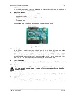
The EV9790 serves as a demonstrator for the CMX979, a 40-lead VQFN device at location U5. 
EV9790 functionality includes: 


2700 - 3600 MHz VCO and 16- / 24-bit Fractional-N PLL 


IF VCO and Integer-N PLL centred at 900MHz 


19.2MHz or optional 38.4MHz VCTCXO, plus external reference input 


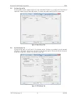
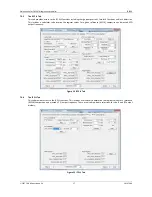
USB Interface via a PE0003 to a CML standard GUI, to allow script control 


7.1


Hardware Description 

Full details of the silicon functionality are contained in the CMX979 datasheet. The EV9790 is assembled on a 65 x 69mm, 
1.6mm thick 6-layer PCB (reference PCB596B), with the upper layer having a Rogers RO4003C ceramic substrate for low 
loss and consistent high frequency performance.  The other layers use FR4 / VT481 2116 dielectric. 
 
In general, RF components, connectors and configuration links have been placed on the top layer, with voltage regulators, 
supplies and decoupling for the CMX979 on the bottom layer. The layout has been optimised for low ground impedance 
and  short  RF  tracking  for  operation  at  high  frequencies.    Gerber  files  and  a  BOM  can  be  downloaded  from  the  CML 
website. 
 
A high frequency SMA edge connector is used for the J1 output with a Grounded Co-Planar Wave Guide transmission line. 
 

7.1.1


RF VCO /PLL 

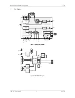
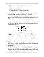
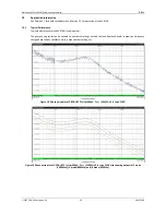
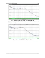
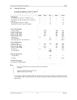
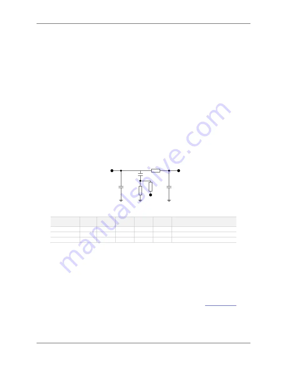
The CMX979 contains a 16- or 24-bit Fractional-N PLL synthesiser used with the on-chip 2700 – 3600 MHz VCO. The loop 
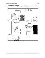
filter is external to the IC and can (optionally) incorporate a fast locking function, see Figure 8. The loop filter output is 
then  routed  back  to  the  tuning  input  of  the  internal  VCO,.  The  on-chip  VCO  output  is  available  off-chip  either  as  a 
fundamental or divided by 2, 4, 6 or 8 at J1. 
 

C14

C3//

C6

C5

R11

R13

DORF

DOIN

FLCK 

(Optional )

R8

(optional)


Figure 8  Example External Components – VCO External Low Pass Filter 


VCO 

Frequency 

C5 

C3//C6 

C14 

R11 

R13 

R8 

(optional FLCK)


2.925GHz 

750pF 

6.2nF 

27pF 

1.6k


5.1k


See Datasheet section 7.3.4 

3.5GHz 

470pF 

3.6nF 

22pF 

2.4k


6.8k


See Datasheet section 7.3.4 

Values Fitted 

680pF 

5.6nF 

27pF 

2.2k


5.6k


See Datasheet section 7.3.4 

 
Note:  C3, C5, C14, R11 and R13 assume a Kvco=70MHz/V, Icp=400uA, Fref=19.2MHz. The values fitted are a compromise 
for  mid-band  operation.  These  values  may  require  modification  for  use  with  other  comparison  frequencies  and  charge 
pump currents.


Table 7  3

rd

 Order Loop Filter Values for a VCO Frequency of 2.925GHz/3.5GHz 

7.1.2


IF PLL/VCO 

The  CMX979  incorporates  an  additional  internal  IF  VCO  and  PLL with  internal  loop  filter.  The  VCO  is  tuned  by  external 
inductor L3; with the default value fitted the tuning range is centred around 900MHz. The VCO output is available either 
as a fundamental or divided by 4, 8 or 16 at the SMA connector J6. 
 

7.1.3


Reference Oscillator 

U4 is a GTXO-91T/EI 19.2MHz 0.5 ppm TCXO, part number MP05955, supplied by Golledge (

www.golledge.com

). This is 

used as the reference for the RF and IF PLLs within the CMX979 (MCLK). Options are provided to use a lower phase noise 
Golledge GTXO-74V/JI 38.4MHz VCTCXO reference, part number MP07489 (footprint U3) or an external reference signal 
can be applied to the SMA connector J3. These inputs can also be buffered via U2. The selection of this buffering is via the 
link configuration field J2. The VCTCXO tuning inputs can be accessed via test loops TL2 and TL4, to allow the addition of a 
modulating signal within the PLL bandwidth. Note that if the alternative oscillator footprint U3 is used, both the supply 
resistor R22 and output coupling capacitor C23 should be removed to disable the unused oscillator U4. 

Summary of Contents for EV9790

Page 1: ...rate integer N IF PLL and VCO covering 500 to 1000 MHz as supplied are also provided An inductor value change can configure the IF VCO to cover other frequency ranges Both VCO outputs can be routed via selectable on chip frequency dividers The board includes all necessary voltage regulators and is operated from an external 6V dc supply The EV9790 provides a 19 2MHz reference oscillator along with ...

Page 2: ...3 2 The C BUS Control Extended Tabs C BUS Ctrl Ext 1 Ext 2 15 7 3 3 The General Control Tab 16 7 3 4 The VCO Calibration Tab 16 7 3 5 The RF PLL Tab 17 7 3 6 The IF PLL Tab 17 7 3 7 The Script Handler Tab 18 7 4 Application Information 20 7 4 1 Typical Performance 20 7 5 Troubleshooting 23 7 5 1 RF PLL Operation 23 7 5 2 IF PLL Operation 23 8 Performance Specification 24 8 1 Electrical Performance...

Page 3: ...omp 19 2MHz PLL type 1100 also showing output in 2 mode 1600MHz 4 mode 800MHz and 8 mode 400MHz 20 Figure 20 Phase noise plot of 3 6GHz RF PLL Icp 400µA FComp 19 2MHz PLL type 1100 21 Figure 21 Phase noise plot of 900MHz IF PLL Icp 400µA FComp 1 2MHz 21 Figure 22 Phase noise plot of 900MHz IF PLL Icp 400µA FComp 1 2MHz also showing the effects of selecting the 4 225MHz 8 112 5MHz and 16 56 25MHz o...

Page 4: ...RF VCC_CP LOOUT DMGND DEC_IFVCO FLCK DEC_LO IRQN VCC_IF_DEC VCC_PLL_CP_IF VCC_SYNTH_3V Divide by 1 2 4 6 or 8 Divide by 1 4 8 or 16 Control Registers DEC_SYNTH IF Synthesiser RF Synthesiser Figure 1 CMX979 Block Diagram C BUS interface Power VREG VREG VCTCXO IF tank Ext Clk IN IF PLL OUT RF PLL OUT Loop filter Modulation J7 J5 AVDD DVDD U5 L3 J2 U3 U4 J3 C BUS CMX979 RF PLL and VCO IF PLL and VCO ...

Page 5: ... J15 although the additional components for this L7 and R41 are not fitted as standard If these components are fitted an external supply should not be connected to J7 In order to apply an external supply with J15 fitted L7 and R41 should be removed Alternatively the PE0003 could be run from the 6 0V supply 4 2 Handling Precautions Like most evaluation kits this product is designed for use in offic...

Page 6: ...lowing procedure is recommended 1 Connect the boards as shown in Figure 5 Note that the HB0003 Interface Board supplied needs to be connected between the PE0003 and EV9790 boards 2 Ensure that the power supply and reference oscillator selection links are correctly configured 3 LO Output signals from the RFPLL can be monitored by a spectrum analyser connected to J1 4 Output from the IF VCO PLL can ...

Page 7: ...pulled high by R48 2 CSN O P Chip Select 3 N C No Connection 4 CDATA O P Command Data 5 N C No Connection 6 SCLK O P Serial Clock 7 N C No Connection 8 RDATA I P Reply Data 9 N C No Connection 10 IRQN I P Interrupt Request open drain 11 GNDD Power Connection to Digital Ground 12 GNDD Power Connection to Digital Ground 13 to 20 N C No Connection Table 2 External C BUS Host Interface CONNECTOR PINOU...

Page 8: ...alogue Ground TL7 AGND Connection to Analogue Ground TL8 DGND Connection to Digital Ground Table 5 Test Loops JUMPERS Ref Default Setting Description JP2 Linked AVDD Analogue Supply Link to enable VCTCXO and buffer supplies JP3 Linked AVDD_979 Link to enable CMX979 analogue supplies JP5 Linked DVDD Link to enable CMX979 digital supplies C BUS interface J2 Link pin 1 2 and pin 3 4 2 x 4 Pin field f...

Page 9: ... 9 UM9790 1 6 Circuit Schematics and Board Layouts For clarity the circuit schematic diagrams are available as separate high resolution files which can be downloaded from the CML website The layout on each side of the PCB is shown in Figure 6 and Figure 7 Figure 6 PCB Layout Top ...

Page 10: ...Evaluation Kit for CMX979 engineering samples EV9790 2017 CML Microsystems Plc 10 UM9790 1 Figure 7 PCB Layout Bottom ...

Page 11: ... or divided by 2 4 6 or 8 at J1 C14 C3 C6 C5 R11 R13 DORF DOIN FLCK Optional R8 optional Figure 8 Example External Components VCO External Low Pass Filter VCO Frequency C5 C3 C6 C14 R11 R13 R8 optional FLCK 2 925GHz 750pF 6 2nF 27pF 1 6k 5 1k See Datasheet section 7 3 4 3 5GHz 470pF 3 6nF 22pF 2 4k 6 8k See Datasheet section 7 3 4 Values Fitted 680pF 5 6nF 27pF 2 2k 5 6k See Datasheet section 7 3 ...

Page 12: ...mentarily at power up Diode D1 is to discharge the capacitor quickly when powering down the board 7 1 6 C BUS Interface The C BUS interface of the CMX979 operates at 1 8V nominal logic levels As a result a level translation interface is required between this and the 3V logic of the PE0003 host controller if used A HB0003 interface is supplied with the EV9790 and provides this function The EV9790 s...

Page 13: ...owing registration to the hard drive of your host PC Extract the files to the hard drive of your host PC Connect a dc supply to the PE0003 Universal Interface Card and set supply voltage level to 5V 500mA current limit Connect a dc supply to the EV9790 and set the voltage level to 6V 250mA current limit Attach a USB cable between the PE0003 Universal Interface Card and the USB port of the PC Turn ...

Page 14: ...into the Address and Data edit boxes is checked to ensure that it is a valid hexadecimal value The radio buttons select an 8 bit or 16 bit read write operation The lengths of the entered values are limited to 2 characters 1 byte for read or write register addresses and 2 or 4 characters 1 or 2 bytes for the register write data The General Reset button writes 00H to the CMX979 device Figure 10 C BU...

Page 15: ... all or Wr Rd all buttons Click on the Wr all button to write all the selected write type C BUS registers Click on the Rd all button to read all the selected read type C BUS registers Click on the Wr Rd all button to read or write all of the selected C BUS registers Two separate tabs are used as one may be used to control a device on the other PE0003 C BUS port Figure 11 C BUS Control Extended Tab...

Page 16: ...ice Status register This tab can also provide control of the RF LO output divider Figure 12 General Control Tab 7 3 4 The VCO Calibration Tab This tab provides access to the RF and IF VCO calibration controls Tick boxes are available to provide automatic calibration or alternatively fixed values can be written to the appropriate registers The returned calibration values can be read back along with...

Page 17: ...is includes a calculator to determine the register values for a given reference MCLK comparison and wanted VCO output frequency Figure 14 RF PLL Tab 7 3 6 The IF PLL Tab This tab provides access to the IF PLL functions This includes a calculator to determine the register values for a reference MCLK comparison and wanted VCO output frequency There are also drop down selections for the IF and RF out...

Page 18: ...uA charge pump current Both IF VCO and bias calibrations are performed and the results displayed For additional confidence the PLL divider registers are also read back To select a script file click on the Select Script button The Open File Dialog is displayed Browse and select the script file The folder that contains the script file will be the working folder of the script i e all the files refere...

Page 19: ...Dialog Box Click on the or buttons to upload and display the next or previous C BUS transaction data block Click on the Read button to upload and display the C BUS transaction data block starting at the address displayed in the Trace Start Address edit box Use the Save button to save the trace data to a file ...

Page 20: ...ce for the EV9790 is shown below The phase noise profiles can be varied by a number of settings notably the loop filter bandwidth comparison frequency charge pump current reference noise output divider setting etc Figure 18 Phase noise plot of 2 8GHz RF PLL Icp 400µA FComp 19 2MHz PLL type 1100 Figure 19 Phase noise plot of 3 2GHz RF PLL Icp 400µA FComp 19 2MHz PLL type 1100 also showing output in...

Page 21: ...Phase noise plot of 3 6GHz RF PLL Icp 400µA FComp 19 2MHz PLL type 1100 The IF PLL has a typical phase noise profile as shown in the plots below using the default L3 inductor value The effect of the divider is demonstrated in Figure 22 Figure 21 Phase noise plot of 900MHz IF PLL Icp 400µA FComp 1 2MHz ...

Page 22: ...X979 engineering samples EV9790 2017 CML Microsystems Plc 22 UM9790 1 Figure 22 Phase noise plot of 900MHz IF PLL Icp 400µA FComp 1 2MHz also showing the effects of selecting the 4 225MHz 8 112 5MHz and 16 56 25MHz outputs ...

Page 23: ... Loop instability The programmed PLL values may give a high gain peak Check the loop components fitted and reprogram with a higher charge pump current or comparison frequency VCO not close to programmed frequency Not calibrated Run auto calibration of the RFVCO and bias using the VCO calibration tab Check continuity of the loop filter Incorrect programming Check that the correct output division ra...

Page 24: ...eding these maximum ratings can result in damage to the Evaluation Kit Min Max Units Supply VIN VSS 0 8 0 V Current into or out of VIN and VSS pins 0 0 5 A Current into or out of any other connector pin 20 20 mA Maximum Input Level 10 dBm 8 1 2 Operating Limits Correct operation of the Evaluation Kit outside these limits is not implied Notes Min Max Units Supply VIN VSS 5 5 8 0 V ...

Page 25: ...450 MHz RF output J1 2 3 7 dBm Output Impedance 50 Phase Noise typical at MHz 10kHz offset TBD dBc Hz IF PLL VCO Parameters Frequency Range 4 700 900 1000 MHz Divide by 4 Output Range 175 250 MHz Divide by 8 Output Range 87 5 125 MHz Divide by 16 Output Range 43 75 62 5 MHz RF output J6 2 3 10 dBm Output Impedance High8k 0 6pF Reference input Ext Clk Input Impedance High Sensitivity 5 20 dBm Micro...

Page 26: ... not permitted within the European Community All software firmware is supplied as is and is without warranty It forms part of the product supplied and is licensed for use only with this product for the purpose of demonstrating the operation of CML products Whilst all reasonable efforts are made to ensure that software firmware contained in this product is virus free CML accepts no responsibility w...

Reviews: