


Evaluation Kit for CMX979 (engineering samples)
EV9790
2017 CML Microsystems Plc
12
UM9790/1
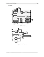
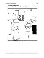
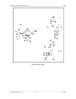
7.1.4
Power Supplies
The input to the PCB is nominally 6.0V (absolute limits: 5.5V to 8V) applied to J7. Reverse polarity protection is provided
by D2. On-board regulators (U6, U8) are provided to generate the 3.3V and 1.8V supplies used on the EV9790.
A green
LED on the digital supply (D3) confirms that power is correctly applied.
7.1.5
Reset Circuit
An RC circuit is provided (R33, C33) to hold the RESETN pin low momentarily at power-up. Diode D1 is to discharge the
capacitor quickly when powering down the board.
7.1.6
C-BUS Interface
The C-BUS interface of the CMX979 operates at 1.8V nominal logic levels. As a result, a level translation interface is
required between this and the 3V logic of the PE0003 host controller, if used. A HB0003 interface is supplied with the
EV9790 and provides this function.
The EV9790 should not be directly connected to the PE0003 C-BUS, otherwise internal damage to the CMX979 could
result.
7.1.7
Inductors
All inductors used in the RF sections of the design are manufactured by Coilcraft (www.coilcraft.com). Performance of the
circuits with inductors from other manufacturers may vary.


