


Evaluation Kit for CMX979 (engineering samples)
EV9790
2017 CML Microsystems Plc
18
UM9790/1
7.3.7
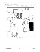
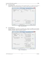
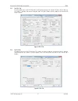
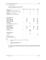
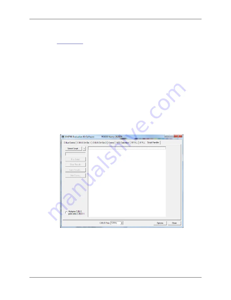
The Script Handler Tab
The Script Handler tab allows the execution of scripts. These are plain text files on the host PC which are compiled by the
GUI, but executed on the ARM Microprocessor on the PE0003
.
The script language is documented separately in the
“Script Language Reference” document, which can be downloaded with the PE0003 support package from the CML
website at
www.cmlmicro.com
.
The following are two demonstration scripts developed for the EV9790 Evaluation Kit:
EV9790_RFPLL 3G2 19M2.pes
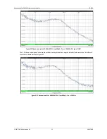
This script locks the RF VCO / PLL at 3.2GHz using the ‘1100’ 16-bit Fractional-N mode with the output at 1.6GHz
(divide by 2 output enabled). A 19.2MHz comparison frequency is used with 400µA charge pump current. Both RF
VCO and bias calibrations are performed and the results displayed. For additional confidence, the PLL divider
registers are also read back.
EV9790_IFPLL.pes
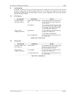
This script locks the IF VCO / PLL at 901.2MHz. A 1.2MHz comparison frequency is used with 400uA charge pump
current. Both IF VCO and bias calibrations are performed and the results displayed. For additional confidence, the
PLL divider registers are also read back.
To select a script file, click on the ‘Select Script’ button. The Open File Dialog is displayed. Browse and select the script file.
The folder that contains the script file will be the working folder of the script (i.e. all the files referenced in the script will
be searched in this folder). Alternatively, select a script file from the recent files list. Click on the ‘>’ button to display the
list.
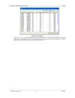
The results window displays the values returned by the script. These results can be saved to a text file or discarded by
clicking on the ‘Save Results’ or ‘Clear Results’ buttons, respectively. When a script file is being executed, the ‘Run Script’
button will change to be the ‘Abort’ button, the rest of the tab will be disabled and the other tabs cannot be selected.
Figure 16 Script Handler Tab
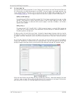
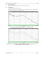
After a script has finished running and when trace data is available, the ‘See Trace…’ button will be enabled. Click on the
‘See Trace…’ button to display the Trace dialog box. Note that the C-BUS transactions are only logged if the feature has
been enabled in the script. See the “Script Language Reference” document for details.


