


Evaluation Kit for CMX979 (engineering samples)
EV9790
2017 CML Microsystems Plc
8
UM9790/1
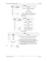
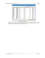
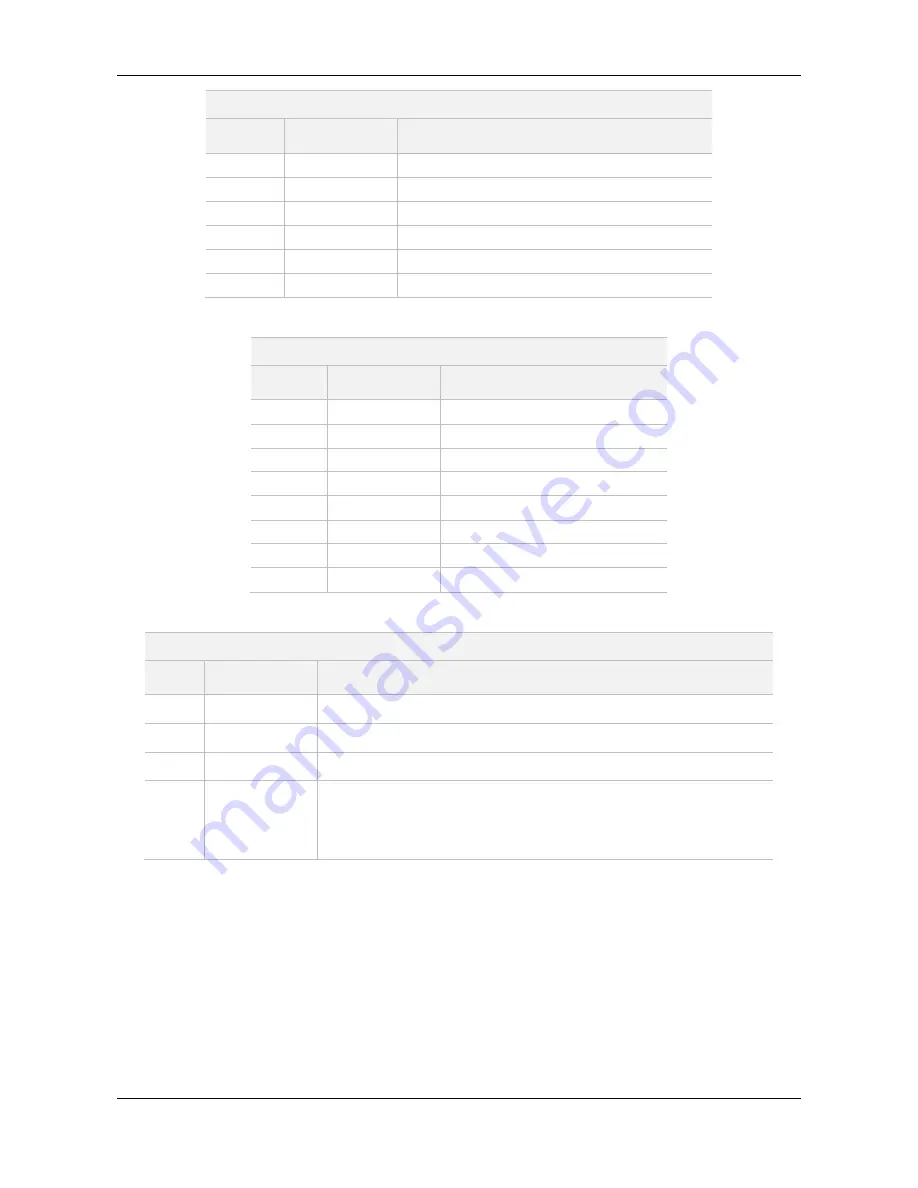
TEST POINTS
Test Point
Ref.
Default
Measurement
Description
TP1
-
DORF – RF PLL Charge pump output voltage
TP3
-
VBIAS
TP4
-
VCC_PLL_CP_IF
TP5
-
+V Input supply voltage
TP6
3.3V
U6 Regulator Output (AVDD) for analogue supplies
TP8
3.3V
U8 Regulator Output (DVDD) for digital supplies
Table 4 Test Points
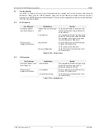
TEST LOOPS
Test Point
Ref.
Default
Measurement
Description
TL1
FLCK – Fast Lock output
TL2
Modulation input for VCTCXO U3
TL3
IRQN
TL4
Modulation input for VCTCXO U4
TL5
RDATA
TL6
AGND
Connection to Analogue Ground
TL7
AGND
Connection to Analogue Ground
TL8
DGND
Connection to Digital Ground
Table 5 Test Loops
JUMPERS
Ref.
Default
Setting
Description
JP2
Linked
AVDD – Analogue Supply - Link to enable VCTCXO and buffer supplies
JP3
Linked
AVDD_979 – Link to enable CMX979 analogue supplies
JP5
Linked
DVDD – Link to enable CMX979 digital supplies (C-BUS interface)
J2
Link pin 1 – 2 and
pin 3 – 4
2 x 4 Pin field for selecting the clock reference source and buffering options
To use the on-board VCTCXO, un-buffered, link pins 1-2 & 3-4.
To use the on-board VCTCXO, buffered, link pins 2-4 & 7-8.
To use an external clock applied to J7, un-buffered, link pins 5-6 & 3-4.
To use an external clock applied to J7, buffered, link pins 4-6 & 7-8.
Table 6 Jumpers
Notes:
I/P
=
Input
O/P
=
Output
TL
=
Test Loop
TP
=
Test Point