background image

LV-669 User’s Manual                                     I/O Port Pin Assignment 

CRT Port 

49 

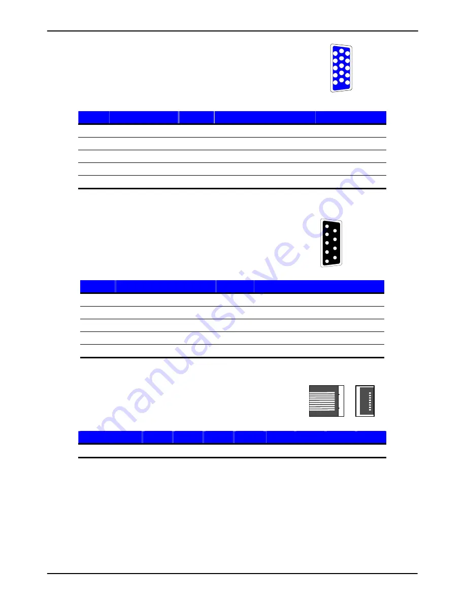
A.4 < CRT Port > 


Connector: CRT 
Type: 15-pin D-sub female connector on panel 

Pin 

Description

Pin

Description

Pin

Description

1 RED 

6  Ground 

11  N/C 

2 GREEN 

7  Ground 

12  5VCDA 

3 BLUE 

8  Ground 

13  HSYNC 

4 N/C 

9  LVGA5V  14  VSYNC 

5 Ground 

10  Ground 

15  5VCLK 


A.5 <Serial Port> 

 
Connector: 

COM1/2


Type: 9-pin D-sub male connector on rear panel 

Pin 

Description 

Pin

Description 

1 DCD 

6 DSR 

2 SIN 

7 RTS 

3 SO 

8 CTS 

4 DTR 

9 RI 

5 Ground 


A.6 <LAN Port> 

Connector:

 RJ45_1/2


Type: RJ45 connector with LED on rear panel 
 

Pin 

Description TX+

TX-

RX+

N/C  N/C

RX-

N/C

N/C


1
2
3
4
5

11

12
13

14

15

6


10

1

8

5
4
3
2
1

9
8
7
6

Summary of Contents for LV-669

Page 1: ...LV 669 Mini ITX Motherboard User s Manual Edition 1 1 2007 07 30...

Page 2: ...ent are property of their respective owners Disclaimer The company shall not be liable for any incidental or consequential damages resulting from the performance or use of this product The company doe...

Page 3: ...otherboard x 1 Cable Kit Printed Matters User s Manual x 1 Driver CD x 1 44 pin ATA33 IDE Cable x 1 40 pin ATA100 IDE Cable x 1 I O Shield SATA Cable x 1 Serial ATA Ribbon Cable x 2 26 pin Slim Type F...

Page 4: ...nce 15 2 3 1 Internal Connector 15 2 3 2 External Connector 15 2 4 CPU and Memory Setup 16 2 4 1 CPU 16 2 4 2 Memory 16 2 5 CMOS ATX Setup 17 2 7 Serial ATA Interface 19 2 8 Floppy Port 20 2 9 LAN Int...

Page 5: ...9 Chapter 4 BIOS Setup 44 Appendix A I O Port Pin Assignment 46 A 1 IDE Port 46 A 2 Floppy Port 48 A 3 Serial ATA Port 48 A 4 CRT Port 49 A 5 Serial Port 49 A 6 LAN Port 49 Appendix B Flash BIOS 50 B...

Page 6: ...LV 669 User s Manual 6 The Page is Left For Blank...

Page 7: ...0 two serial ATA ports with RAID array function 6 x USB2 0 ports and 5 1 channel AC97 audio Multimedia solution Based on VIA CN700 chipset the board provides 18 24 bit LVDS interface or DVI which supp...

Page 8: ...ard One Compact Flash Type II socket on solder side Serial ATA VIA VT8237R Plus integrates 2 Serial ATA interface RAID 0 1 array Technology supported Multi I O Port Chipset VIA VT8237R Plus with Winbo...

Page 9: ...cket support Mini PCI typeII IEEE1394 One IEEE 1394 connector on rear I O Panel Power and Environment Power Requirement DC 12V input with external DC Jack or onboard 4 pin connector 8 24V DC input Dim...

Page 10: ...LV 669 User s Manual Introduction Mechanical Drawing 10 1 3 Mechanical Drawing...

Page 11: ...GA2 1 x 184 pin DDR333 400 Up to 1GB CRT LCD Monitor VT1636 LVDS CN700 VT8237R Ultra V Link 533MB s 6 x USB2 0 Ports PCI 2 x 8110S 32 2 x LAN 2 x SATA AC97 ALC655 4 x Serial ports 1 x Floppy port 8 bi...

Page 12: ...are Setup Connector Location 12 Chapter 2 Hardware Setup 2 1 Connector Location CN_DIO DC_OUT DIMM CN_LPT CPUFAN CN_COM3 4 CN_DVI CN_LVDS FDD SATA1 2 CN_INV IDE2 IDE1 MINIPCI PCI CN_USB SYSFAN JFRNT C...

Page 13: ...LV 669 User s Manual Hardware Setup Connector Location 13 CF IEEE1394 PS2 COM1 2 CRT AUDIO USB_RJ45_1 2 DC_IN...

Page 14: ...2 Jumper Reference Jumper Function JRTC CMOS Operating Clear Setting JCFSEL Compact Flash address mode setting JVLCD LCD Panel Voltage Setting LV 669X only JAT AT ATX mode setting JCSEL1 2 COM2 RS232...

Page 15: ...ystem cooler fan connector Standard CN_COM3 4 5 x 2 pin RS232 serial port Standard CF Compact Flash Type II socket Standard CN_LVDS 20 x 2 pin LVDS LCD interface LV669X Only Slim CN_INV 5 pin LCD inve...

Page 16: ...supports VIA C7 processor default ratio is C7 1 5G with cooler 2 4 2 Memory The board supports one 184 pin DDR333 400 SDRAM and up to 1GB of capacity only non ECC unbuffered memory is supported 80 pi...

Page 17: ...refuses to boot due to inappropriate CMOS settings here is how to proceed to clear reset the CMOS to its default values Jumper JRTC Type Onboard 3 pin jumper JRTC Mode 1 2 Clear CMOS 2 3 Normal Opera...

Page 18: ...API devices with ATA33 66 100 133 Based on embedded application the board has one 44 pin IDE connector 5V supported for disk on module The board also provides a Compact Flash Type II socket with jumpe...

Page 19: ...following is the list of the specification of the Serial ATA 1 Complies with Serial ATA Specification Revision 1 0 2 Dual Channel master mode PCI 3 On chip two channel Serial ATA S ATA PHY for support...

Page 20: ...please use the 26 pin ribbon cable in the package to connect the floppy device 4 Lift up this plastic bar 5 Slot the cable in Blue paste for outside 6 Press back the plastic bar Floppy rear side 1 Lif...

Page 21: ...al Hardware Setup LAN Interface 21 2 9 LAN Interface The board provides Two GigaLAN interfaces with REALTEK 8110S 32 PCI controller and compliant with standard IEEE 802 3 Ethernet interface for 100BAS...

Page 22: ...d Display Interface Based on VIA CN700 the board supports integrated S3 Graphics UniChrome Pro IGP graphics with BIOS selectable 16 32 64MB shared with system memory for frame buffer 2 10 1 Analog VGA...

Page 23: ...Digital Display The board provides one 40 pin LVDS connector for 18 24 bit dual channel panels supports up to 1600 x 1200 UXGA of resolution with one LCD backlight inverter connector and one jumper fo...

Page 24: ...CC3 3 3 4 GND 5 ENABKL Connector CN_LVDS Type onboard 40 pin connector for LVDS connector Connector model HIROSE DF13 40DP 1 25V Pin Signal Pin Signal 2 LCDVCC 1 LCDVCC 4 GND 3 GND 6 ATX0 5 BTX0 8 ATX...

Page 25: ...to make a cable because every panel has its own pin assignment so we do not provide a standard cable please find a local cable manufacture to make cables LCD Installation Guide 1 Preparing the LV 669...

Page 26: ...BIOS panel type selection form VGA ROM VERSION 9Y 9X 00 20 NO Resolution Color Channel 0 640 x 480 18 1 1 800 x 600 18 1 2 1024 x 768 18 1 3 1280 x 768 18 1 4 1280 x 1024 24 1 5 1400 x 1050 18 2 6 160...

Page 27: ...Realteck ALC655 Connector CN_AUDIO Type 10 pin 2 x 5 header pitch 2 54mm Pin Description Pin Description 1 Line SURR Left 2 Ground 3 Line SURR Right 4 MIC1 CEN 5 MIC2 LEF 6 Ground 7 N C 8 Line Out Le...

Page 28: ...8 2 12 USB2 0 Interface Based on VIA VT8237R Plus the board provides 6 USB2 0 ports The USB2 0 interface provides up to 480Mbps of transferring rate Interface USB2 0 Controller VIA VT8237R Transfer Ra...

Page 29: ...3 Data0 4 Data1 5 Data0 6 Data1 7 Ground 8 Ground 9 Ground 10 N C PS The USB2 0 will be only active when you connecting with the USB2 0 devices if you insert an USB1 1 device the port will be changed...

Page 30: ...mable 8 bit digital I O interface you can use this general purpose I O port for system control like POS or KIOSK Connector CN_DIO Type onboard 2 x 6 pin header pitch 2 0mm Pin Description Pin Descript...

Page 31: ...ovides three RS232 serial ports with jumper selectable RS422 485 for CN_COM4 Connector CN_COM3 4 Type 10 pin 5 x 2 header for COM3 4 Pin Description Pin Description 1 DCD 422RX 485 2 RXD 422RX 485 3 T...

Page 32: ...LV 669 User s Manual Hardware Setup Serial Port Jumper Setting 32 COM1 2 CN_COM3 4 JCSEL2 JCSEL1 10 1...

Page 33: ...nnector for DC 8 24V input it also has one 4 pin P4 additional use power connector for internal power supply you can choose one of them to meet your application 2 15 1 Power Input Connector CN_12V Typ...

Page 34: ...tput Pin Description Pin Description Pin Description Pin Description 1 5V 2 Ground 3 Ground 4 12V Note Maximum output voltage 12V 5A 5V 3A 2 15 3 Fan Connector Connector CPUFAN SYSFAN Type 3 pin fan w...

Page 35: ...button reset and beeper etc Please check well before you connecting the cables on the chassis Connector JFRNT Type onboard 14 pin 2 x 7 2 54 pitch header Function Signal PIN Signal Function HDLED 1 2...

Page 36: ...LV 669 User s Manual 36 This Page is Left For Blank...

Page 37: ...the data from first drive to second drive for data security and if one drive fails the system would access the applications to the workable drive It needs two unused drives or one used and one unused...

Page 38: ...Configuration 38 You also can edit disk array under OS please install the VIA RAID Utility in the driver CD To getting start please click here to learn more information Click here to build RAID 0 Clic...

Page 39: ...dio interface with driver installed please install the Realtek ALC655 audio driver in the CD before getting start to enjoy the 5 1 channel sound system 1 Install REALTEK AC97 Audio driver 2 Lunch the...

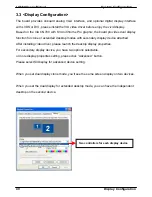
Page 40: ...lone or extended desktop modes with secondary display device attached After installing video driver please launch the desktop display properties For secondary display device you have two options selec...

Page 41: ...LV 669 User s Manual System Configuration Display Configuration 41 There are two options for secondary display device For more display properties setting please click Advanced button...

Page 42: ...ce setting When you set dual display clone mode you ll see the same screen display on two devices When you set the dual display for extended desktop mode you can have the independent desktop on the se...

Page 43: ...LV 669 User s Manual 43 This Page is Left for Blank...

Page 44: ...ormation when the power is turned off If the battery runs out of the power then the settings of BIOS will come back to the default setting The BIOS section of the manual is subject to change without n...

Page 45: ...LV 669 User s Manual 45 This Page is Left for Blank...

Page 46: ...ion Pin Description 1 Reset 2 Ground 3 D7 4 D8 5 D6 6 D9 7 D5 8 D10 9 D4 10 D11 11 D3 12 D12 13 D2 14 D13 15 D1 16 D14 17 D0 18 D15 19 Ground 20 VCC 21 REQ 22 Ground 23 IOW STOP 24 Ground 25 IOR HDMAR...

Page 47: ...Ground 3 D7 4 D8 5 D6 6 D9 7 D5 8 D10 9 D4 10 D11 11 D3 12 D12 13 D2 14 D13 15 D1 16 D14 17 D0 18 D15 19 Ground 20 N C 21 REQ 22 Ground 23 IOW STOP 24 Ground 25 IOR HDMARDY 26 Ground 27 IORDY DDMARDY...

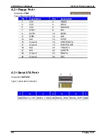
Page 48: ...2 INDEX 3 VCC 4 DRV0 5 VCC 6 DSKCHG 7 DRV1 8 N C 9 MTR1 10 MTR0 11 RPM 12 DIR 13 N C 14 STEP 15 Ground 16 WRITE DATA 17 Ground 18 WRITE GATE 19 N C 20 TRACK 0 21 N C 22 WRPTR 23 Ground 24 RDATA 25 Gro...

Page 49: ...LUE 8 Ground 13 HSYNC 4 N C 9 LVGA5V 14 VSYNC 5 Ground 10 Ground 15 5VCLK A 5 Serial Port Connector COM1 2 Type 9 pin D sub male connector on rear panel Pin Description Pin Description 1 DCD 6 DSR 2 S...

Page 50: ...ame of the tool is awdflash exe it s the utility that can write the data into the BIOS flash ship and update the BIOS B 2 Flash Method 1 Please make a bootable floppy disk 2 Get the last bin files you...

Page 51: ...LV 669 User s Manual System Resources I O Port Address Map 51 Appendix C System Resources C1 I O Port Address Map...

Page 52: ...LV 669 User s Manual System Resources I O Port Address Map 52...

Page 53: ...LV 669 User s Manual System Resources Memory Address Map 53 C2 Memory Address Map...

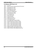
Page 54: ...LV 669 User s Manual System Resources System IRQ Resources 54 C3 System IRQ Resources...

Page 55: ...r configuration o 4E 87 o 4E 2A o 4F FD enable GPIO function o 4E 07 o 4F 07 enable GPIO configuration o 4E F0 o 4F xx set GPIO as input output set 1 for input 0 for output o 4E F1 o 4F xx if set GPIO...

Page 56: ...p as system reset mode by program Timeout Value Range 1 to 255 Second or Minute Program Sample Watchdog timer setup as system reset with 5 second of timeout 2E 87 2E 87 2E 07 2F 08 Logical Device 8 2E...

Page 57: ...LV 669 User s Manual 57 This Page is Left for Blank...

Page 58: ...with us We will do our best to support you for your products projects and business Taiwan Commate Computer Inc Address 8F No 94 Sec 1 Shin Tai Wu Rd Shi Chih Taipei Hsien Taiwan TEL 886 2 26963909 FA...

Reviews: