background image

LV-67I User’s Manual                                                                                                             


Copyright 


Copyright 2009. All rights reserved. This document is copyrighted and all rights are 
reserved. The information in this document is subject to change without prior notice to make 
improvements to the products. 
This document contains proprietary information and protected by copyright. No part of this 
document may be reproduced, copied, or translated in any form or any means without prior 
written permission of the manufacturer. 
All trademarks and/or registered trademarks contains in this document are property of their 
respective owners. 

Disclaimer 


The company shall not be liable for any incidental or consequential damages resulting from 
the performance or use of this product. 
The company does not issue a warranty of any kind, express or implied, including without 
limitation implied warranties of merchantability or fitness for a particular purpose. 
The company has the right to revise the manual or include changes in the specifications of 
the product described within it at any time without notice and without obligation to notify any 
person of such revision or changes. 


Trademark 


All trademarks are the property of their respective holders. 


Any questions please visit our website at 

http://www.commell.com.tw

Summary of Contents for LV-67I

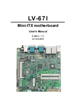
Page 1: ...LV 67I Mini ITX motherboard User s Manual Edition 1 0 2012 04 09 ...

Page 2: ...cument are property of their respective owners Disclaimer The company shall not be liable for any incidental or consequential damages resulting from the performance or use of this product The company does not issue a warranty of any kind express or implied including without limitation implied warranties of merchantability or fitness for a particular purpose The company has the right to revise the ...

Page 3: ...se our products Hardware LV 67I Mini ITX motherboard x 1 Cable Kit SATA Cable x 1 OALSATA L DC Power Cable x 1 OALDC 2 ATX Power Output Cable x 1 OALATX P3S2 COM port Printer Port Cable x 1 OALES BKU 3 DVI Module With DVI Cable x 1 BADPDVI A OALDVI DF13 I O Shieldx 1 OPLATE LV67I ...

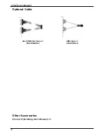
Page 4: ...LV 67I User s Manual 4 USB Cable x 1 OALUSBA 3 Dual COM Port Cable x 1 OALES BKU2 Optional Cable Other Accessories Divers CD including User s Manual x 1 ...

Page 5: ...nal Connectors 15 2 3 2 External Connectors 15 2 4 Memory Setup 16 2 5 CMOS ATX Setup 17 2 6 Serial ATA Interface 18 2 7 Network Interface 19 2 8 Onboard Display Interface 20 2 8 1 Analog Display 20 2 8 2 Digital Display Interface 21 2 9 Audio Interface 25 2 10 GPIO and SMBUS Interface 27 2 11 USB Interface 28 2 12 Power Supply and Fan Interface 30 2 12 1 Power Input 30 2 12 2 Power Output 31 2 12...

Page 6: ... GPIO Port 45 A 4 USB Interface 46 A 5 Serial Port 46 A 6 Parallel Port 47 A 7 VGA Port 47 A 8 LAN Port 48 A 9 SMBus 48 Appedix B System Resources 49 B 1 I O Port Address Map 49 B 2 Memory Address Map 51 B 3 System IRQ Resources 52 B 4 System DMA Resources 56 Appedix C Flash BIOS 57 C 1 BIOS Auto Flash Tool 57 C 2 Flash Method 57 Appendix D Programming GPIO s 58 Appendix E Watch Dog timer Setting ...

Page 7: ...LV 67I User s Manual 7 This Page is Left for Blank ...

Page 8: ...r The Intel Atom N2800 Dual core processor is with 1 86GHz clock Speed 1MB L2 cache It s built on 32nm process technology support Hyper Threading Technology Enhanced Intel Speedstep Technology Intel 64 Intel NM10 Chipset The board integrates Intel NM10 The chipset features power efficient graphics with an integrated 32 bit 3D graphics engine based on Intel Graphics Media Accelerator 3650 architect...

Page 9: ...rts SIR K B Mouse External PS 2 keyboard and mouse ports on rear I O panel GPIO One 12 pin Digital I O connector with 8 bit programmable I O Interface Smart Fan One CPU fan connectors for fan speed controllable VGA Display Interface Chipset Intel integrated extreme GMA 3650 Display Type CRT LCD monitor with analog display single channel LVDS Connector External DB15 female connector on rear I O pan...

Page 10: ...hin 0 60 O p C 32 140 O p F Storage within 20 85O p C 4 185 O p F Ordering Code LV 67ID Support Intel Atom D2700 processor with onboard VGA LVDS for 18 and 24 bits DVI Audio Giga LAN USB2 0 SATAII PCIE mini card PCI Mini PCI Serial Port CF SMBUS GPIO IrDA LPT CDIN SPDIF LV 67IN Support Intel Atom N2800 processor with onboard VGA LVDS for 18 bits DVI Audio Giga LAN USB2 0 SATAII PCIE mini card PCI ...

Page 11: ... SO DIMM 4GB max W83627DHG P 18 24bit Single Channel LVDS CRT DVI 6 x USB2 0 port 2 x serial ATAII D2700 N2800 Intel Atom NM10 1 x PCIE mini card socket Mini PCI Slot PCI Slot 4 x Serial Port ICHF81216D ALC888 HD Audio 2 x Serial Port 2 x PCIE Giga LAN GPIO IrDA LPT ...

Page 12: ...LV 67I User s Manual 12 1 4 Mechanical Drawing ...

Page 13: ...ardware Setup 2 1 Connector Location PS2 CN_LVDS CN_INV CN_12V CPUFAN CN_COM4 CN DIO SYSFAN JFRNT CN_AUDIO CDIN CN_IR ATX DDRIII S_ATA1 2 PCI Mini PCI Mini Card CN_LPT CN_SMBUS CN_USB1 2 CN_LPC CN_DVI CN_COM5 6 S A COM3 COM2 udio PDIF USB_RJ45_1 2 COM1 CRT ...

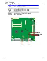
Page 14: ...C CMOS Operating Clear Setting JVLCD Panel Voltage Setting JP39 COM3 signal mode switch For Pin 9 JP49 COM4 signal mode switch For Pin 9 JAT Power mode select JCSEL1 JCSEL2 CN_COM2 RS 232 RS422 RS485 Setting CN_IR IrDA Setting JRTC JCSEL2 JCSEL1 JP39 JP49 JAT JVLCD ...

Page 15: ...tem cooler fan connector CN_IR 5 pin IrDA connector CN_COM4 5 x 2 pin RS232 CN_COM56 10 x 2 pin 2 x RS232 CN_LPT 13 x 2 pin printer connector CN_SMBUS 5 pin SMBUS connector CN_INV 5 pin LCD inverter connector CN_LVDS 10 x 2 pin LVDS connector CN_DVI 10 x 2 pin DVI connector JFRNT 14 pin front panel switch indicator connector PCI 120 Pin PCI socket Mini PCI 124 pin Mini PCI socket MINI_CARD 52 pin ...

Page 16: ... ECC unbuffered memory is supported only LV67I provides two 204 pin DDR3 SO DIMM to support DDR3 800 1066 memory modules support up to 4GB of capacity Suggestion DDR3 SO DIMM Modules Raw Card C Single sided x 8 Raw Card F Double sided x 8 DDRIII ...

Page 17: ...o boot due to inappropriate CMOS settings here is how to proceed to clear reset the CMOS to its default values Jumper JRTC Type Onboard 3 pin jumper JRTC Mode 1 2 Clear CMOS 2 3 Normal Operation Default setting Jumper JAT Type onboard 3 pin jumper JAT Mode 1 2 AT Mode 2 3 ATX Mode Default setting 3 1 JAT JRTC 1 3 ...

Page 18: ...LV 67I User s Manual 18 2 6 Serial ATA Interface Based on Intel NM10 the board provides Three Serial ATAII interfaces with up to 300MB s of transfer rate S_ATA1 2 ...

Page 19: ...9 2 7 Network Interface The board integrates with two Intel 82583V Gigabit Ethernet controllers as the PCI Express bus The Intel 82583V supports triple speed of 10 100 1000Base T with IEEE802 3 compliance and Wake On LAN supported LAN2 LAN1 ...

Page 20: ...CD backlight inverter connector The board provides dual display function with clone mode and extended desktop mode for CRT and LVDS Notice When you install any PCI Graphic card the onboard graphics would be disabled automatically 2 8 1 Analog Display Please connect your CRT or LCD monitor with DB15 male connector to the onboard DB15 female connector on rear I O port LV 67I supports 1920 x 1200 WUX...

Page 21: ...e 20 pin LVDS connector for 18 bit single channel panels LV 67IN supports 1366 x 768 WUXGA of resolution and LV 67ID supports 1400 x 900 WUXGA of resolution with one LCD backlight inverter connector and one jumper for panel voltage setting 1 5 CN_INV CN_LVDS 1 19 2 20 1 3 JVLCD ...

Page 22: ...on Pin Description 1 12V 1 2 5V 2 CTLBKL 2 3 3 3V 3 GND Default 2 3 4 GND 5 ENABKL Connector CN_LVDS Type onboard 20 pin connector for LVDS connector Connector model HIROSE DF13 20DP 1 25V Pin Signal Pin Signal 2 LCDVCC 1 LCDVCC 4 GND 3 GND 6 TXL0P 5 TXL0N 8 TXL1N 7 GND 10 GND 9 TXL1P 12 TXL2P 11 TXL2N 14 TXLCKN 13 GND 16 GND 15 TXLCKP 18 TXL3P 17 TXL3N 20 GND 19 GND ...

Page 23: ...le because every panel has its own pin assignment so we do not provide a standard cable please find a local cable manufacture to make cables LCD Installation Guide 1 Preparing the LV 67I LCD panel and the backlight inverter 2 Please check the datasheet of the panel to see the voltage of the panel and set the jumper JVLCD to 5V or 3 3V 3 You would need a LVDS type cable Panel side Board side For sa...

Page 24: ... you need to select the LCD panel type in the BIOS The panel type mapping is list below LV 67I BIOS panel type selection form On board Single channel LVDS 18bit NO Output format 1 640 x 480 2 800 x 600 3 1024 x 768 4 1280 x 1024 5 1366 x 768 6 1280 x 800 ...

Page 25: ... compliance The main specifications of ALC888 are z High performance DACs with 100dB S N ratio z 2 DAC channels support 16 20 24 bit PCM format for 2 audio solution z 16 20 24 bit S PDIF OUT supports 44 1K 48K 96kHz sample rate z Compatible with HD z Meets Microsoft WHQL WLP 2 0 audio requirements The board provides 2 channels audio phone jacks on rear I O port Line in MIC in ports for front I O p...

Page 26: ...4mm Pin Description Pin Description 1 MIC2_L 2 Ground 3 MIC2_R 4 AVCC 5 FP_OUT_R 6 MIC2_JD 7 SENSE 8 N C 9 FP_OUT_L 10 LINE2_JD Connector CDIN Type 4 pin header pitch 2 54mm Pin Description 1 CD Left 2 Ground 3 Ground 4 CD Right SPDIF MIC IN LINE IN LINE OUT Rear I O phone jacks ...

Page 27: ...terface for control panel application Connector CN_DIO Type onboard 2 x 6 pin header pitch 2 0mm Pin Description Pin Description 1 Ground 2 Ground 3 GP10 4 GP14 5 GP11 6 GP15 7 GP12 8 GP16 9 GP13 10 GP17 11 5V 12 12V 5 CN_SMBUS 12 CN_DIO 1 1 11 2 Connector CN_SMBUS Type 5 pin header for SMBUS Ports Pin Description 1 5V 2 N C 3 SMBDATA 4 SMBCLK 5 Ground ...

Page 28: ...ow Interface USB2 0 Controller Intel NM10 Transfer Rate Up to 480Mb s Voltage 5V The Intel NM10 contains one Enhanced Host Controller Interface EHCI and four Universal Host Controller Interfaces UHCI it can determine whether your connected device is for USB1 1 or USB2 0 and change the transfer rate automatically USB3 4 5 6 ...

Page 29: ... User s Manual 29 Connector CN_USB1 2 Type 10 pin 5 x 2 header for USB5 6 Ports Pin Description Pin Description 1 VCC 2 VCC 3 Data0 4 Data1 5 Data0 6 Data1 7 Ground 8 Ground 9 Ground 10 N C 1 9 2 10 CN_USB1 2 ...

Page 30: ...tion report on appendix Connector ATX It also can become Output when DC IN be used Type 20 pin ATX power connector Pin Assignment Pin Assignment 1 3 3V 11 3 3V 2 3 3V 12 12V 3 GND 13 GND 4 5V 14 PSON 5 GND 15 GND 6 5V 16 GND 7 GND 17 GND 8 PW_OK 18 N C 9 5V_SB 19 5V 10 12V 20 5V DC_IN 4 3 11 1 20 10 ATX 1 2 Connector DC_IN Type 4 pin standard Pentium 4 additional 9 24V power connector Pin Descript...

Page 31: ...en DC IN had power supplied the ATX become output Avoid DC IN and ATX power supply input at the same time Connector ATX When DC IN be used Type 20 pin ATX connector for 3 3V 5V 12V Output Pin Assignment Pin Assignment 1 3 3V 11 3 3V 2 3 3V 12 3 13 4 5V 14 5 GND 15 6 16 GND 7 GND 17 GND 8 18 9 19 5V 10 12V 20 5V Note Maximum output voltage 12V 2A 5V 3A 3 3V 2A ATX ...

Page 32: ...ler and one 3 pin cooler fan connectors for system SYSFAN 1 3 1 4 CPUFAN Connector CPUFAN Type 4 pin fan wafer connector Pin Description Pin Description 1 Ground 2 12V 3 Fan Speed Detection 4 Fan Control Connector SYSFAN Type 3 pin fan wafer connector Pin Description Pin Description Pin Description 1 Ground 2 12V 3 Sense ...

Page 33: ...RS232 422 485 serial ports The jumper JCSEL1 JCSEL2 can let you configure the communicating modes for COM2 COM1 COM3 COM2 Connector COM2 Type 9 pin D sub male connector on bracket for COM2 Pin Description Pin Description 1 DCD 422TX 485 2 RXD 422TX 485 3 TXD 422RX 4 DTR 422RX 5 GND 6 DSR 7 RTS 8 CTS 9 RI 10 N C ...

Page 34: ...LV 67I User s Manual 34 Setting RS 232 RS 422 RS 485 for COM2 1 2 8 7 JCSEL2 1 9 2 19 1 CN_COM5 6 CN_COM4 1 2 JP39 JP49 1 2 1 2 11 JCSEL1 12 20 2 10 ...

Page 35: ...2 7 1 1 11 8 2 12 2 RS 485 RS 232 11 1 Jumper JP39 JP49 COM3 4 Type onboard 6 pin header 1 2 8 7 1 2 8 7 12 2 1 11 12 2 Default setting JCSEL1 1 3 2 4 7 9 8 10 JCSEL2 1 2 Power Mode JP39 JP49 Pin 9 with 5V Power 1 2 Pin 9 with 12V Power 3 4 Default setting 5 6 5 1 6 2 5 1 6 2 ...

Page 36: ...r etc Please check well before you connecting the cables on the chassis Connector JFRNT Type onboard 14 pin 2 x 7 2 54 pitch header Function Signal PIN Signal Function HDLED 1 2 PWDLED IDE LED HDLED 3 4 N C Reset 5 6 PWDLED Power LED Reset Reset 7 8 SPKIN N C 9 10 N C PWRBT 11 12 N C Power Button PWRBT 13 14 SPKIN Speaker 14 1 JFRNT 2 13 ...

Page 37: ...LV 67I User s Manual 37 This Page is Left for Blank ...

Page 38: ...board integrates Intel NM10 with REALTEK ALC888 codec It can support 2 channel sound under system configuration Please follow the steps below to setup your sound system 1 Install REALTEK HD Audio driver 2 Lunch the control panel and Sound Effect Manager 3 Select Speaker Configuration ...

Page 39: ...LV 67I User s Manual 39 4 Select the sound mode to meet your speaker system ...

Page 40: ...700 N2800 with GMA3650 Graphic Media Accelerator the board supports two DACs for display device as different resolution and color bit Please install the Intel Graphic Driver before you starting setup display devices 1 Click right button on the desktop to lunch Screen Resolution ...

Page 41: ...LV 67I User s Manual 41 2 Click Advanced button for more specificity setup Click Graphics Properties for advanced setup ...

Page 42: ...anual 42 3 This setup options can let you define each device settings Click Monitor to setup the CRT monitor for Resolution and Refresh Rate Click Intel Dual Display Clone to setup the dual display mode as same screen ...

Page 43: ...ion when the power is turned off If the battery runs out of the power then the settings of BIOS will come back to the default setting The BIOS section of the manual is subject to change without notice and is provided here for reference purpose only The settings and configurations of the BIOS are current at the time of print and therefore they may not be exactly the same as that displayed on your s...

Page 44: ...LV 67I User s Manual 44 This Page is Left for Blank ...

Page 45: ...SATA_TXN1 GND RSATA_RXN1 RSATA_RXP1 GND A 2 IrDA Port Connector CN_IR 1 Type 5 pin header for SIR Ports 5 Pin Description 1 VCC 2 N C 3 IRRX 4 Ground 5 IRTX A 3 GPIO Port Connector CN_DIO Type onboard 2 x 6 pin header pitch 2 0mm Pin Description Pin Description 1 Ground 2 Ground 3 GP10 4 GP14 5 GP11 6 GP15 7 GP12 8 GP16 9 GP13 10 GP17 11 VCC 12 12V 1 11 2 12 ...

Page 46: ...scription Pin Description 1 VCC 2 VCC 3 Data0 4 Data1 5 Data0 6 Data1 7 Ground 8 Ground 9 Ground 10 N C A 5 Serial Port 5 4 3 2 1 9 8 7 6 Connector COM1 2 3 Type 9 pin D sub male connector on bracket Pin Description Pin Description 1 DCD 422TX 485 2 RXD 422TX 485 3 TXD 422RX 4 DTR 422RX 5 GND 6 DSR 7 RTS 8 CTS 9 RI 10 N C ...

Page 47: ... 18 Ground 6 PRO4 19 Ground 7 PRO5 20 I O Ground 8 PRO6 21 Ground 9 PRO7 22 Ground 10 ACK 23 Ground 11 BUSY 24 Ground 12 PE 25 Ground 13 SLCT 26 N C A 7 VGA Port 5 1 Connector CRT1 10 6 Type 15 pin D sub female connector on bracket 15 11 Pin Description Pin Description Pin Description 1 RED 6 Ground 11 N C 2 GREEN 7 Ground 12 DDC_DA 3 BLUE 8 Ground 13 HSYNC 4 N C 9 5V 14 VSYNC 5 Ground 10 Ground 1...

Page 48: ... Type RJ45 connector with LED on rear panel Pin 1 2 3 4 5 6 7 8 Description TRD0 TRD0 TRD1 TRD2 TRD2 TRD1 TRD3 TRD3 A 9 SMBus Connector CN_SMBUS Type 4 pin SMBus connector Pin Description Pin Description 1 VCC 2 N C 3 SMBDATA 4 SMBCLK 5 Ground 1 5 5 CN_SMBUS 1 ...

Page 49: ...LV 67I User s Manual 49 Appedix B System Resources B 1 I O Port Address Map ...

Page 50: ...LV 67I User s Manual 50 ...

Page 51: ...LV 67I User s Manual 51 B 2 Memory Address Map ...

Page 52: ...LV 67I User s Manual 52 B 3 System IRQ Resources ...

Page 53: ...LV 67I User s Manual 53 ...

Page 54: ...LV 67I User s Manual 54 ...

Page 55: ...LV 67I User s Manual 55 ...

Page 56: ...LV 67I User s Manual 56 B 4 System DMA Resources ...

Page 57: ... is awdflash exe it s the utility that can write the data into the BIOS flash ship and update the BIOS C 2 Flash Method 1 Please make a bootable floppy disk 2 Get the last bin files you want to update and copy it into the disk 3 Copy awardflash exe to the disk 4 Power on the system and flash the BIOS Example C awardflash XXX bin 5 Re star the system Any question about the BIOS re flash please cont...

Page 58: ... 87 o 2E 07 o 2F 09 enable GPIO function o 2E 30 o 2F 02 enable GPIO configuration o 2E F0 o 2F xx set GPIO as input output set 1 for input 0 for output o 2E F1 o 2F xx if set GPIO s as output in this register its value can be set Optional o 2E F2 o 2F xx Data inversion register 1 inverts the current valus of the bits 0 leaves them as they are o 2E 30 o 2F 01 active GPIO s For further information ...

Page 59: ...by program Timeout Value Range 1 to 255 Second or Minute Program Sample Watchdog timer setup as system reset with 5 second of timeout 2E 87 2E 87 2E 07 2F 08 Logical Device 8 2E 30 Activate 2F 01 2E F5 Set as Second 2F 00 2E F6 Set as 5 2F 05 Minute bit 3 0 Second bit 3 1 You can select Timer setting in the BIOS after setting the time options the system will reset according to the period of your s...

Page 60: ...l do our best to support you for your products projects and business Taiwan Commate Computer Inc Address 19F No 94 Sec 1 Shin Tai Wu Rd Shi Chih Taipei Hsien Taiwan TEL 886 2 26963909 FAX 886 2 26963911 Website http www commell com tw E Mail info commell com tw General Information tech commell com tw Technical Support Commell is a brand name of Taiwan commate computer Inc ...

Reviews: