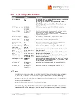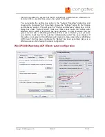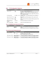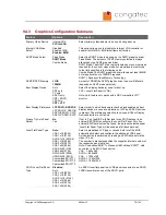
7.9 Boot Strap Signals
Table 35
Boot Strap signal Descriptions
Signal
Description of Boot Strap
Signals
I/O
PU/PD
Comment
REQ1..3#
Bus request
I 3.3V
PU 8k2 3.3V REQ1..3# is a boot strap signal (see
caution statement below)
GNT2/3#
Bus grant
O 3.3V
GNT2/3# are boot strap signals (see
note below)
SATALED#
Serial ATA Led. Open collector
output pin driven during SATA
command activity.
OC 3.3V
SATALED# is a boot strap signal (see
caution statement below)
PCI_GNT#A
reserved
O 3.3V
PCI_GNT#A is a boot strap signal
(see note below)
AC_SYNC
Serial Bus Synchronization.
O 3.3V
AC_SYNC is a boot strap signal (see
caution statement below)
AC_SDOUT
Audio Serial Data Output to
CODEC.
O 3.3V
AC_SDOUT is a boot strap signal
(see caution statement below)
DTR1#
Data terminal ready for COM1
O 5V
PU 4k7 5V
DTR1# is a boot strap signal (see
caution statement below)
TXD1, TXD2
Data transmit for COM1/COM2 O 5V
PU 4k7 5V
TXD1 and TXD2 are boot strap
signals (see caution statement below)
RTS1#
Request to send for COM1
O 5V
PD 4k7
RTS1# is a boot strap signal (see
caution statement below)
SPEAKER
Speaker output
O 3.3V
SPEAKER is a boot strap signal (see
caution statement below)
SDVOCTRL_DATA
I²C based control signal (Data)
for SDVO device.
SDVOCTRL_DATA is a boot strap
signal. Pulled high indicates an
external SDVO application is present.
Caution
The signals listed in the table above are used as chipset configuration straps during
system reset. In this condition (during reset), they are inputs that are pulled to the
correct state by either XTX
™
internally implemented resistors or chipset internally
implemented resistors that are located on the module. No external DC loads or external
pull-up or pull-down resistors should change the configuration of the signals listed in the
above table with the exception of AC_SYNC, AC_SDOUT and SDVOCTRL_DATA.
External resistors may override the internal strap states and cause the XTX
™
module to
malfunction and/or cause irreparable damage to the module.
AC_SYNC and AC_SDOUT can be used to switch PCI Express channels 0-3 between
x1 and x4 mode. If both signals are each pulled-up (using 1k Ω resistors) to 3.3V at the
rising edge of PWROK then x4 mode is enabled. x1 mode is used by default if these
resistors are not populated. SDVOCTRL_DATA can be pulled-up (using 5.6KΩ resistor)
to 2.5V in order to tell the chipset to run in SDVO mode.
If it is necessary to drive a TTL input (or another input which sources or sinks significant
current) that uses the TXD1 signal, a CMOS-input buffer can be inserted in the signal
path so that this line is not pulled up or down by external circuitry during system reset.
Copyright © 2006 congatec AG
X945m13
64/102


