4. Functions
ADA16-32/2(PCI)F
55
Conversion data
The following equation represents the relationship between input data and voltage.
Voltage = Input data x (Max. range value – Min. range value) / Reso Min. range value
The value of resolution for the 12-bit device is 4096; that for the 16-bit device is 65536.
The table below shows the relationship between input data and voltage in the ±10-V range.
Voltage
Conversion data (12-bit)
Voltage
Conversion data (16-bit)
+9.995V
4095 +9.99970V
65535
:
: :
:
0.005V
2049 0.00030V
32769
0V
2048 0V
32768
-0.005V
2047 -0.00030V
32767
:
: :
:
-10.000V
0 -10.000V
0
Ex.: When input data 3072 is input at a resolution of 12-bit in the ± 10-V range
Voltage = 3072 x (10 - (-10)) ÷ 4096 + (-10)
=
5.0
4.Reset
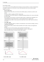
Various states can be reset by executing the following reset commands:
Status
This command resets the sampling clock error status and AD conversion error status.
Memory
This can only be used when the transfer mode is set to device buffer mode.
This command resets the following memory related states.
-
Resets the conversion data in memory.
-
Resets the repeat count to 0.
-
Resets the sampling count to 0 when a stop trigger is input.
-
Resets the buffer overflow status.
-
Resets the status information for the specified data save count.
Summary of Contents for ADA16-32/2(PCI)F
Page 7: ...vi ADA16 32 2 PCI F ...
Page 33: ...2 Setup 26 ADA16 32 2 PCI F ...
Page 45: ...3 External Connection 38 ADA16 32 2 PCI F ...
Page 99: ...5 About Software 92 ADA16 32 2 PCI F ...
Page 108: ......


