background image

5. Each Component Function 


66


BX-320 User’s manual 

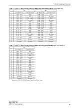
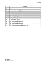
Table 5.14. F&eIT I/F pin assignments 

No. 

Signal 

Dir 

Description 

No. 

Signal 

Dir 

Description 

x86 

x86 

A01  FG 

  Frame ground 

B01  FG 

  Frame ground 

A02  N.C. 

  Not connected 

B02  N.C. 

  Not connected 

A03  SA15 

OUT 

Address bus 15 

B03  SA14 

OUT 

Address bus 14 

A04  SA13 

OUT 

Address bus 13 

B04  SA12 

OUT 

Address bus 12 

A05  SA11 

OUT 

Address bus 11 

B05  SA10 

OUT 

Address bus 10 

A06  SA09 

OUT 

Address bus 09 

B06  SA08 

OUT 

Address bus 08 

A07  SA07 

OUT 

Address bus 07 

B07  SA06 

OUT 

Address bus 06 

A08  SA05 

OUT 

Address bus 05 

B08  SA04 

OUT 

Address bus 04 

A09  SA03 

OUT 

Address bus 03 

B09  SA02 

OUT 

Address bus 02 

A10  SA01 

OUT 

Address bus 01 

B10  SA00 

OUT 

Address bus 00 

A11  RESERVED   

Reserved 

B11  RESERVED   

Reserved 

A12  RESERVED 

  Reserved 

B12  RST_x86# 

IN 

CPU reset signal 

A13  SD00 

IN/OUT  Data bus 00 

B13  SD01 

IN/OUT  Data bus 01 

A14  SD02 

IN/OUT  Data bus 02 

B14  SD03 

IN/OUT  Data bus 03 

A15  SD04 

IN/OUT  Data bus 04 

B15  SD05 

IN/OUT  Data bus 05 

A16  SD06 

IN/OUT  Data bus 06 

B16  SD07 

IN/OUT  Data bus 07 

A17  SD08 

IN/OUT  Data bus 08 

B17  SD09 

IN/OUT  Data bus 09 

A18  SD10 

IN/OUT  Data bus 10 

B18  SD11 

IN/OUT  Data bus 11 

A19  SD12 

IN/OUT  Data bus 12 

B19  SD13 

IN/OUT  Data bus 13 

A20  SD14 

IN/OUT  Data bus 14 

B20  SD15 

IN/OUT  Data bus 15 

A21  GND 

  Ground 

B21  GND 

  Ground 

A22  AEN 

OUT 

Address enable signal 

B22  IOCHCK# 

IN 

NMI signal 

A23  IOR# 

OUT 

Read signal 

B23  IRQ7 

IN 

Interrupt signal 

A24  IOW# 

OUT 

Write signal 

B24  IRQ5 

IN 

Interrupt signal 

A25  GND 

  Ground 

B25  GND 

  Ground 

A26  CLK8MHz 

OUT 

Bus clock 

B26  IO_RST# 

OUT 

Reset signal 

A27  GND 

  Ground 

B27  CPUSEN 

OUT 

CPU ID 

A28  IOCHRDY# 

IN/OUT  Wait signal 

B28  GND 

  Ground 

A29  GND 

  Ground 

B29  GND 

  Ground 

A30  RESETDRV 

  ISA RESETDRV signal 

B30  RESERVED 

  Reserved 

A31  IRQ9 

IN 

Interrupt signal 

B31  RESERVED 

  Reserved 

A32  RESERVED   

Reserved 

B32  RESERVED 

  Reserved 

A33  SBHE 

IN/OUT  ISA SBHE signal 

B33  IOCS16# 

IN 

ISA IOCS16 signal 

A34  RESERVED 

  Reserved 

B34  RESERVED 

  Reserved 

A35  RESERVED 

  Reserved 

B35  RESERVED 

  Reserved 

A36  RESERVED 

  Reserved 

B36  RESERVED 

  Reserved 

A37  VCC 

  +5.0V power supply 

B37  VCC 

  +5.0V power supply 

A38  VCC 

  +5.0V power supply 

B38  VCC 

  +5.0V power supply 

A39  VCC 

  +5.0V power supply 

B39  VCC 

  +5.0V power supply 

A40  VCC 

  +5.0V power supply 

B40  VCC 

  +5.0V power supply 

Remarks) 

The symbol "#" at the end of an item represents negative logic. In an I/O module, normally a pin is reset by using pin B26 
IO_RST#. The signal B27 CPUSEN indicates a Low level output. The IRQx signal represents a signal for which the rise 
edge is enabled. Total power ratings for the power supply pins: 5.0VDC, 3.0A. 

Summary of Contents for BX-320-DC700000

Page 1: ...IPC Series BOX PC for BX 320 Series User s Manual CONTEC CO LTD...

Page 2: ...removal prevention fitting 1 1 CFast card removal prevention fitting bottom face side 1 2 1 2 Cable clamp 1 1 Power connector 1 1 Product guide this sheet 1 1 IPC Precaution List 1 1 Warranty Certifi...

Page 3: ...in this document is subject to change without notice All relevant issues have been considered in the preparation of this document Should you notice an omission or any questionable item in this docume...

Page 4: ...8 2 SYSTEM REFERENCE 9 Specifications 9 Power Management Features 11 Power Requirements 12 Power Consumption 12 Physical Dimensions 13 3 HARDWARE SETUP 15 Before Using the Product for the First Time 1...

Page 5: ...on 38 CSM Configuration 39 Chipset 40 North Bridge 41 Intel IGD Configuration 42 South Bridge Configuration 44 Azalia HD Audio Configuration 45 Security 48 Secure Boot menu 50 Boot Configuration 51 Sa...

Page 6: ...hernet LAN A B 61 CFast Card Connector CFast1 62 Serial Port Interface SERIAL A B 63 BUS EXPANDER PCIe 64 F IT I F 65 6 APPENDIX 71 POST Codes 71 Interrupt Level List 74 SERIAL I O Address and Registe...

Page 7: ...vi BX 320 User s manual...

Page 8: ...uct utilizes the Intel Atom Processor E3845 for the CPU This product is equipped with an external expansion connector that can be connected by cable to an expansion chassis for PCI PCI Express expansi...

Page 9: ...rge operational labor savings Freely expandable peripherals Twin CFast card slots and other abundant interfaces This product is equipped with expandable interfaces including 1000BASE T x 2 USB 3 0 x 1...

Page 10: ...TSB 2016 64bit Japanese English Chinese Korean 2 10 or more than it of a main frame BIOS version is an operating conditions of Windows 10 Support Software You should use CONTEC support software accord...

Page 11: ...this device is returned freight prepaid with a copy of the original invoice and a Return Merchandise Authorization to the distributor or the CONTEC group office from which it was purchased This warran...

Page 12: ...Precautions Always check that the power supply is turned off before connecting or disconnecting power cables Do not modify the product Always turn off the power before inserting or removing circuit b...

Page 13: ...onnector Always remove the power cable from the power outlet before connecting or disconnecting a connector To prevent corruption of files always shutdown the OS before turning off this product CONTEC...

Page 14: ...ent This equipment generates uses and can radiate radio frequency energy and if not installed and used in accordance with the instruction manual may cause harmful interference to radio communications...

Page 15: ...operations Security measures e g Do not keep using the default password Refer to the product manual for the password setting Set a strong password Combined with upper and lowercase letters and numbers...

Page 16: ...TX 10BASE T 2 port Wake On LAN support USB USB 3 0 compliant 1 port USB 2 0 compliant 3 port Serial I F RS 232C general purpose 2port SERIAL PORTA B 9pin D SUB connector male Baud rate 50 115 200bps W...

Page 17: ...connector x3 RS 232C 2 port 9pin D SUB connector male F eIT 3 1 port PCI Express cable 1 port 18pin PCI Express External Cabling connector Power supply Rated input voltage 12 24VDC 4 Range of input v...

Page 18: ...spheric discharge 8kV IEC61000 4 2 Level 3 EN61000 4 2 Level 3 Vibration resistance Sweep resistance 10 57Hz semi amplitude 0 15 mm 57 150Hz 2 0G 40 min each in x y and z directions JIS C60068 2 6 com...

Page 19: ...akes sure your power supply provides a range of 10 8 V minimum to 31 2 V maximum DC power source Power Consumption For typical configurations the CPU card is designed to operate with at least a 60W po...

Page 20: ...p and bottom and 4 mm or lower for the back Figure 2 1 BX 320 DCxxxxxx Including screw hole dimensions 1 2 To secure this product with the included fittings use the included screws M3x7 In other situa...

Page 21: ...2 System Reference 14 BX 320 User s manual...

Page 22: ...eps 1 and 2 turn on the power If you find any abnormality after turning on the power turn it off and check to see if the setup has been performed properly STEP4 Set up BIOS By referring to Chapter 4 s...

Page 23: ...f screws are tightened with a torque greater than the specified torque The specified tightening torque is 5 6kgf cm If you use a CFast card other than the optional card we cannot guarantee the specifi...

Page 24: ...guarantee the specifications of this product To use the product within its specifications be sure to use the optional CFast card To prevent potential damage caused by static electricity take appropria...

Page 25: ...he module onto this product using the bundled F eIT module fixing parts If a stack connector protective cover is attached the connection operation should be performed after the cover is removed Figure...

Page 26: ...the main unit Figure 3 5 Removing a DIN Rail Installation Metal Fittings 1 2 2 Remove the bundled countersunk screws Figure 3 6 Removing a DIN Rail Installation Metal Fittings 2 2 Screw holes may be d...

Page 27: ...the fixing hook with a flat head screw driver the fixing hook can be locked This should be done on all connected device modules 3 Hook the unit an object consisting of a controller and a module from t...

Page 28: ...evice module is connected pull down the fixing hook of the device module to unlock it This should be done on all connected device modules Figure 3 8 Removing the module from the DIN rail 1 2 2 With th...

Page 29: ...such as those from vibrations and impacts secure the cable to the connector with the included cable clamp as shown in the figure below use the four included M3x7 screws Figure 3 9 Attaching the cable...

Page 30: ...ng temperature 0 50 C 1 When using 1000BASE T 0 45 C Installable directions at operating temperature 0 35 C 2 When using 1000BASE T 0 30 C Installable directions that is unusable 3 4 5 6 Figure 3 11 I...

Page 31: ...3 Hardware Setup 24 BX 320 User s manual Distances between this product and its vicinity Figure 3 12 Distances between this product and its vicinity...

Page 32: ...so as not to allow waste heat from the product to accumulate around the product Do not install this product in completely sealed spaces except when it is possible to adjust the internal temperature us...

Page 33: ...rating temperature is decided from the multiple measurement points as shown below When making use of the product the air current should be adjusted to prevent that all the temperatures measured at the...

Page 34: ...contained in the FLASH ROM and begins the process of checking out the system and configuring it When it finishes the BIOS will seek an operating system on one of the disks and then launch and turn co...

Page 35: ...ROM and exit An attention when using Windows 10 The attention at the time of making default configuration by BIOS other than making OS reinstallation recovery Please be sure to use the CSM Support se...

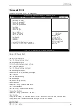
Page 36: ...ersion 00 05 00 00 TXE FW Version 01 01 00 1089 System Language English System Date Week Day MM DD YYYY System Time HH MM SS Access Level Administrator Select Screen Select Item Enter Select Change Op...

Page 37: ...I 1 3 Displays the UEFI version Project Version B320C 0 01 x64 Displays the BIOS version Build Data and Time 03 31 2016 11 31 22 Displays the BIOS creation date and time Access Level Administrator Dis...

Page 38: ...m Enter Select Change Opt F1 General Help F2 Previous Values F3 Optimized Defaults F4 Save Exit ESC Exit Version x xx xxxx Copyright C 20xx American Megatrends Inc Figure 4 2 Advanced Manu ACPI Settin...

Page 39: ...Sleep State Suspend Disabled S3 Suspend to RAM Configure the Sleep State settings Wake On LAN RI Control on S5 Disabled Enabled Set the Wake on LAN Resume on Ring functions These functions cannot be...

Page 40: ...Save Exit ESC Exit Version x xx xxxx Copyright C 20xx American Megatrends Inc Figure 4 4 Super IO Configuration Table 4 6 Super IO Configuration Item Option Description Serial Port A Configuration Re...

Page 41: ...on Description Serial Port Disabled Enabled Configure the operation settings for serial port B Change Settings IO 2F8h IRQ 3 IO 3F8h IRQ 3 4 5 6 7 9 10 11 12 IO 2F8h IRQ 3 4 5 6 7 9 10 11 12 IO 3E8h I...

Page 42: ...lth Status System temperature 35 C CPU temperature 42 C VCORE 0 888 V 1 8V 1 760 V 5V 5 024 V 5VSB 5 056 V 3 3 VSB 3 312 V 3 3 VCC 3 296 V VBAT 3 216 V Select Screen Select Item Enter Select Change Op...

Page 43: ...it Enabled Intel Virtualization Technology Disabled Select Screen Select Item Enter Select Change Opt F1 General Help F2 Previous Values F3 Optimized Defaults F4 Save Exit ESC Exit Version x xx xxxx C...

Page 44: ...sabled Select Screen Select Item Enter Select Change Opt F1 General Help F2 Previous Values F3 Optimized Defaults F4 Save Exit ESC Exit Version x xx xxxx Copyright C 20xx American Megatrends Inc Figur...

Page 45: ...t C 20xx American Megatrends Inc Figure 4 8 SATA Configuration Table 4 11 SATA Configuration Item Option Description Serial ATA SATA Enabled Disabled Configure the SATA controller operation settings C...

Page 46: ...I Select Screen Select Item Enter Select Change Opt F1 General Help F2 Previous Values F3 Optimized Defaults F4 Save Exit ESC Exit Version x xx xxxx Copyright C 20xx American Megatrends Inc Figure 4 9...

Page 47: ...orth Bridge South Bridge Select Screen Select Item Enter Select Change Opt F1 General Help F2 Previous Values F3 Optimized Defaults F4 Save Exit ESC Exit Version x xx xxxx Copyright C 20xx American Me...

Page 48: ...U Max TOLUD 3 GB Bypass SPD Detect Disable Select Screen Select Item Enter Select Change Opt F1 General Help F2 Previous Values F3 Optimized Defaults F4 Save Exit ESC Exit Version x xx xxxx Copyright...

Page 49: ...Size 2MB Select Screen Select Item Enter Select Change Opt F1 General Help F2 Previous Values F3 Optimized Defaults F4 Save Exit ESC Exit Version x xx xxxx Copyright C 20xx American Megatrends Inc Fi...

Page 50: ...4 BIOS Setup BX 320 User s manual 43 Item Option Description MAX Aperture Size 128MB 256MB 512MB Do not change this setting GTT Size 1MB 2MB Do not change this setting...

Page 51: ...CH IO Configuration Item Option Description Azalia HD Audio Refer to Table 4 16 USB Configuration Refer to Table 4 17 LAN Configuration Refer to Table 4 18 High Precision Timer Enabled Disabled Config...

Page 52: ...io Controller Enabled Select Screen Select Item Enter Select Change Opt F1 General Help F2 Previous Values F3 Optimized Defaults F4 Save Exit ESC Exit Version x xx xxxx Copyright C 20xx American Megat...

Page 53: ...Configuration Item Option Description Legacy USB Support Enabled Disabled Auto Configure whether USB keyboards and similar devices will be usable with legacy operating systems such as MS DOS XHCI Han...

Page 54: ...ct Item Enter Select Change Opt F1 General Help F2 Previous Values F3 Optimized Defaults F4 Save Exit ESC Exit Version x xx xxxx Copyright C 20xx American Megatrends Inc Figure 4 16 LAN Configuration...

Page 55: ...Secure Boot menu Select Screen Select Item Enter Select Change Opt F1 General Help F2 Previous Values F3 Optimized Defaults F4 Save Exit ESC Exit Version x xx xxxx Copyright C 20xx American Megatrends...

Page 56: ...e Boot menu It is displayed when CSM Support is set as Disabled Leave these settings as configured before shipment Be careful to not forget the password If you forget the password the product will hav...

Page 57: ...oot Not Active Vendor Keys Not Active Secure Boot Enabled Secure Boot Mode Standard Key Management Select Screen Select Item Enter Select Change Opt F1 General Help F2 Previous Values F3 Optimized Def...

Page 58: ...merican Megatrends Inc Figure 4 19 Boot Configuration Table 4 20 Boot Configuration Item Option Description Setup Prompt Timeout 1 Set the standby time for BIOS Setup DEL or F2 input Unit second Bootu...

Page 59: ...oot is performed under the assumption the disk is MBR formatted If 2 is selected a UEFI boot is performed under the assumption the disk is GPT formatted Make sure to specify 1 as the boot setting Boot...

Page 60: ...F4 Save Exit ESC Exit Version x xx xxxx Copyright C 20xx American Megatrends Inc Figure 4 20 Save Exit Saving Changes and Exit Save the changed settings and exit Discard Change and Exit Exit without s...

Page 61: ...4 BIOS Setup 54 BX 320 User s manual...

Page 62: ...5 Each Component Function BX 320 User s manual 55 5 Each Component Function Component Name Front View BX 320 DCxxxxxx Figure 5 1 Component Name...

Page 63: ...rt TYPE A connector x 1 USB2 0 USB2 0 port TYPE A connector x 3 LAN A Ethernet 1000BASE T 100BASE TX 10BASE T RJ 45 connector LAN B Ethernet 1000BASE T 100BASE TX 10BASE T RJ 45 connector CFast1 CFast...

Page 64: ...e ON Green DC Power Input Connector DC IN To supply the power always use the power supply listed below Rated input voltage 12 24VDC Range of input voltage 10 8 31 2VDC Power capacity 12V 4 2A or more...

Page 65: ...ssed This IO port bit is read only User Programmable Switch uSW Reading bit 0 of IO port 8802H indicates the switch state A value of 1 indicates the switch is pressed and 0 indicates no pressed This I...

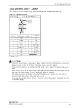
Page 66: ...Analog RGB interface and then the display is connected after the OS boots the display may not be shown properly When the analog display is used Windows MS DOS may not be properly displayed in full scr...

Page 67: ...A interface Table 5 5 USB3 0 Connector Pin No Signal name USB3 0 1 USB_VCC 2 DATA 3 DATA 4 USB_GND 5 SSRX 6 SSRX 7 USB_GND 8 SSTX 9 SSTX USB2 0 Port USB2 0 This product is equipped with 3 channel for...

Page 68: ...3 8 N C TRD 3 Table 5 8 Giga bit Ethernet Connector LED name State Display contents Link LED Right ON Green Indicates that the Normal connection Blinking Green Indicates that the Operation Transmit LE...

Page 69: ...l name Pin No Signal name PC1 CDI S1 GND PC2 GND S2 TX PC3 N C S3 TX PC4 N C S4 GND PC5 N C S5 RX PC6 N C S6 RX PC7 GND S7 GND PC8 LED PC9 N C PC10 N C PC11 N C PC12 N C PC13 3 3V PC14 3 3V PC15 GND P...

Page 70: ...ports independently The same I O address and IRQ cannot be shared with any other device Table 5 10 SERIAL A B I O Addresses and Interrupts SERIAL I O address Interrupt A 3F8h 3FFh IRQ 4 B 2F8h 2FFh I...

Page 71: ...tion 1 Tx PCI Express transmitting line 10 GND GND 2 Tx 11 CPERST Reset signal 3 Reserved None 12 N C None 4 N C None 13 CLK PCI Express clock 5 GND GND 14 CLK 6 Reserved None 15 N C None 7 Reserved N...

Page 72: ...power to be supplied to the F eIT I F is 3A Therefore make sure that the total current consumption of connected modules does not exceed 3A Table 5 13 F eIT I F connector Connector type FX8C 80S SV HI...

Page 73: ...19 SD13 IN OUT Data bus 13 A20 SD14 IN OUT Data bus 14 B20 SD15 IN OUT Data bus 15 A21 GND Ground B21 GND Ground A22 AEN OUT Address enable signal B22 IOCHCK IN NMI signal A23 IOR OUT Read signal B23...

Page 74: ...EN delay time 1 tAEN2 30 IOW delay time 2 tIOW2 100 IOW delay time 1 tIOW1 100 IOW pulse width tIOW 16bit 225 8bit 520 IOCHRDY delay time tRDY1 16bit 75 8bit 360 IOCHRDY pulse width tRDY 125 15600 Dat...

Page 75: ...pulse width tIOR 16bit 160 8bit 520 IOCHRDY delay time tRDY1 16bit 75 8bit 360 IOCHRDY pulse width tRDY 125 15600 Data setup time tRSD1 24 Data hold time tRSD2 45 Figure 5 5 F eIT I F I O read cycle...

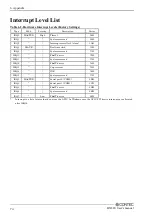
Page 76: ...20 9827 IRQ5 9828 982F IRQ7 A 9840 9847 IRQ7 9848 984F IRQ10 B 9860 9867 Not in use 9868 986F Not in use C 0700 0707 IRQ10 0708 070F IRQ10 D 0720 0727 IRQ7 0728 072F IRQ7 E Reserved Reserved Reserved...

Page 77: ...5 Each Component Function 70 BX 320 User s manual...

Page 78: ...ization Specific South Bridge 1Dh 2Ah OEM PRI memory initialization code 2Bh Memory initialization Serial Presence Detect SPD Data loading 2Ch Memory initialization Memory detection 2Dh Memory initial...

Page 79: ...PCI bus initialization starts 93h PCI bus hot plug controller initialization 94h Enumerate PCI bus number 95h PCI bus resource requests 96h PCI bus resource allocation 97h Console output device conne...

Page 80: ...tem during migration 02h S2 sleep system during migration 03h S3 sleep system during migration 04h S4 sleep system during migration 05h S5 sleep system during migration 10h From S1 sleep state during...

Page 81: ...VE Real time clock 70H IRQ9 System reserved 71H IRQ10 F eIT device 72H IRQ11 System reserved 73H IRQ12 F eIT device 74H IRQ13 Co processor 75H IRQ14 IDE 76H IRQ15 System reserved 77H IRQ3 MASTER Seria...

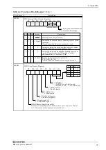
Page 82: ...ster THR R Receive buffer register RBR 1 W Divisor latch register LSB DLL 03F9H 1 W Divisor latch register MSB DLM 0 W Interrupt enable register IER 03FAH X R Interrupt ID register IIR 03FBH X W Line...

Page 83: ...received data from 03F8H DLL Divisor Latch LSB DLAB 1 D7 D6 D5 D4 D3 D2 D1 D0 bit7 MSB bit0 LSB Baud rate setting register LSB 03F8H D7 D6 D5 D4 D3 D2 D1 D0 bit7 MSB bit0 LSB Baud rate setting regist...

Page 84: ...ceiving buffer is read Generated when the transmitter holding register is empty Cleared when the IIR is read or when transmitted data is written to THR Modem status interrupt is generated CTS DSR RI C...

Page 85: ...back test 0 Disable 1 Enable LSR Line Status Regester 03FDH D7 D6 D5 D4 D3 D2 D1 D0 0 TEMT THRE BI FE PE OE DR Data ready 1 for existence of received data Overrun error 1 for occurrence of an error Pa...

Page 86: ...6 D5 D4 D3 D2 D1 D0 03FEH I O address Description SCR Scratchpad Register 03FFH DCD RI DSR CTS DDCD TERI DDSR DCTS Delta CTS Delta DSR Trailing edge RI Delta data carrier detect CTS DSR RI DCD This is...

Page 87: ...d their respective values to be written to the divisor latch register LSB MSB Table 6 5 Baud Rate Settings Baud rate to be set SERIAL A B Clock input 1 8432MHz Value to be set in the divisor register...

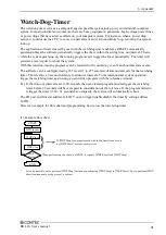
Page 88: ...igured using 255 levels 1 to 255 seconds of timeout intervals for the watchdog timer There is also a 2 second tolerance for timeout intervals To maintain normal system operation trigger the watchdog t...

Page 89: ...nded function mode MOV DX 2EH MOV AL 87H OUT DX AL OUT DX AL Select logical device WDT number 8 MOV DX 2EH MOV AL 07H OUT DX AL MOV DX 2FH MOV AL 08H OUT DX AL Activate logical device WDT number 8 MOV...

Page 90: ...the extended function mode MOV DX 2EH MOV AL 87H OUT DX AL OUT DX AL Select logical device WDT number 8 MOV DX 2EH MOV AL 07H OUT DX AL MOV DX 2FH MOV AL 08H OUT DX AL Set time of WDT and start to cou...

Page 91: ...the extended function mode MOV DX 2EH MOV AL 87H OUT DX AL OUT DX AL Select logical device WDT number 8 MOV DX 2EH MOV AL 07H OUT DX AL MOV DX 2FH MOV AL 08H OUT DX AL Stop count down of WDT MOV DX 2E...

Page 92: ...6 Appendix BX 320 User s manual 85 MOV DX 2EH MOV AL AAH OUT DX AL The timer s intervals have a tolerance of 2 seconds CAUTION...

Page 93: ...ithium content 1g or less Removing the battery Remove the battery according to the following figure 1 Remove the battery according to the following figure As shown in the figure unscrew the 18 screws...

Page 94: ...ment page size KB NAND Flash memory life span cycles The number of management page to be rewritten per 1 cycle Example2 MLC When the file of 4MB is made for CFS 32GBM A and it rewrites it once per 10...

Page 95: ...6 Appendix 88 BX 320 User s manual...

Page 96: ...ast Card CFS 32GBQ A 32GB CFast Card CFS 32GBQ B 32GB CFast Card Higher environmental resistance type PCI Bus Expansion Chassis ECH PCI CE H4D Short size x 4 DIN rail attachment is possible Precaution...

Page 97: ...Osaka 555 0025 Japan Japanese http www contec co jp English http www contec com Chinese http www contec com cn No part of this document may be copied or reproduced in any form by any means without pr...

Reviews: