background image

Appendix B: Cable Pinout Definition Tables

25

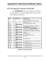
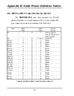
B.3  User Data Port Connector For RS-530

The 

MUX128/2*64

 user data channel for RS-530

physical interface is a 25-pin female D-type connector wired

in accordance with Table B-3.

Abbr.

Pin Direction

Description

FG

1

Chassis ground.
May be isolated from signal ground.

SG

7

Signal Ground.

TD(A)
TD(B)

2

14

To

MUX128/2*64

Serial digital data from DTE.

RD(A)
RD(B)

3

16

From

MUX128/2*64

Serial digital data at the output of the

MUX128/2*64

/2*64K receiver.

RTS(A)
RTS(B)

4

19

To

MUX128/2*64

ON signal to the 

MUX128/2*64

/2*64k

when data transmission is desired.

CTS(A)
CTS(B)

5

13

From

MUX128/2*64

Constantly ON or follow RTS. (DIP SW
setting).

DSR(A)
DSR(B)

6

22

From

MUX128/2*64

Constantly ON,
Except during test loops.

DTR(A)
DTR(B)

20
23

To

MUX128/2*64

Not used.

DCD(A)
DCD(B)

8

10

From

MUX128/2*64

Constantly ON.

ETC(A)
ETC(B)

24
11

To

MUX128/2*64

A transmitted data rate clock input from
the data source.

TC(A)
TC(B)

15
12

From

MUX128/2*64

A transmitted data rate clock for use by an
external data source.

RC(A)
RC(B)

17

9

From

MUX128/2*64

A received data rate clock for use by an
external data source.

Table B-3: RS-530 pin allocation

Summary of Contents for MUX128

Page 1: ...INSTALLATION and OPERATIONMANUAL ...

Page 2: ......

Page 3: ... Installation and Operation 2 1 General 9 2 2 Site Preparation 9 2 3 Mechanical Assembly 9 2 4 Electrical Installation 9 2 5 Dip Switch and Jumper Settings 11 2 6 Front Panel 13 2 7 Loop Back Operation 13 2 8 Auto Delay Feature 16 Chapter 3 Optional Rack Mounting 17 Appendix A DIP Switch Setting Tables 19 A 1 DSW1 Setting Clock Source Setup 19 A 2 DSW2 Setting Data Port Setup 20 A 3 DSW3 Setting D...

Page 4: ...1 DB9 Connectors 23 B 2 User Data Port Connector for RS 232 24 B 3 User Data Port Connector for RS 530 25 B 4 User Data Port Connector for V 35 26 B 5 User Data Port Connector for X 21 27 B 6 User Data Port Connector for RS 449 28 B 7 User Data Port Connector for V 36 29 ...

Page 5: ...ween the two units be less than half of a 64Kbps cycle Figure 1 1 Point to point connection diagram The delay between A CH 64K and B CH 64K should be the same Any delay may be manually nulled via DIP switch settings The delay may also be automatically detected while in Auto Delay mode for automatic nulling In either case for normal operation the delay between channels must remain fixed after setti...

Page 6: ...ceiving side the incoming data is split equally bit for bit to the A and B channels of the G 703 64K interfaces When receiving data from the G 703 channels the data is recombined to form the outputted 128Kbps stream There are 6 interface standards supported by the Data Port They are RS 530 RS 449 X 21 V 35 RS 232 and V 36 The output connector for the Data Port is a standard DB25F connector Interfa...

Page 7: ...etail Co directional The term co directional is used to describe an interface across which the information and its associated timing signal are transmitted in the same direction see Figure 1 4 Figure 1 4 Co directional interface This mode is the most popular for point to point applications All timing modes recovery transparent data port or internal oscillator are possible in this mode Equipment Da...

Page 8: ...ep 3 A binary zero is coded as a block of four bits 1010 Step 4 The binary signal is converted into a three level signal Step 5 A Violation block marks the last bit in an octet The next page displays a figure showing the boundaries for the standard pulse signals for proper operation and compatibility with other G 703 equipment 7 1 8 0 1 3 4 5 1 6 1 7 1 8 0 1 0 1 0 2 0 1 Octet timing Step 5 Step 4 ...

Page 9: ...irectional interface V 0 V 0 3 12 µs 3 9 0 78 3 51 s 3 9 0 39 3 9 s 4 29 µs 3 9 2 6 6 5 µs 3 9 0 39 7 8 µs 3 9 3 9 0 5 1 0 7 02 µs 7 8 0 78 7 41 µs 7 8 0 39 7 8 s 8 19 µs 7 8 2 6 10 4 µs 7 8 0 39 11 7 s 7 8 3 9 1 0 0 5 µ a Mask for single pulse b Mask for double pulse ...

Page 10: ...k Loop back to DTE l Self testing function 1 5 Specifications G 703 Interface Specifications l Type Co directional 64Kbps l Line 4 wires 0 5 0 7mm l Impedance 120 Ω Balanced l Clock frequency 64KHz 100ppm l Complies with ITU G 703 and G 823 jitter l Frame format unframed only l Line code 64Kbps co directional line code l Connector DB9 F proprietary User Data Interface Specifications l Interface Ty...

Page 11: ...attern according to ITU for direct end to end integrity testing The Error indicator flashes for each bit error detected Operation is described in Chapter 2 1 7 Timing Considerations Multiple clock source selection provides maximum flexibility in connecting both the G 703 64K link and user data interface The G 703 64K link may be clocked from the recovered receive clock from the user data port or f...

Page 12: ...ly the timing mode selected for network operation Internal timing The MUX128 2 64 G 703 link transmit clock is derived from the internal clock oscillator This timing mode is necessary in point to point applications over leased lines In this case one MUX128 2 64 must use the internal oscillator and the other must operate from the recovered clock Transparent timing The MUX128 2 64 synchronous data c...

Page 13: ...anical Assembly The MUX128 2 64 is designed for tabletop bench or optional rack mount installation and is delivered completely assembled No provision has been made for bolting the MUX128 2 64 to a tabletop Rack mounting instructions are provided in Chapter 3 2 4 Electrical Installation 2 4 1 Power connection AC power is supplied to the MUX128 2 64 through a standard 3 prong IEC connector Refer to ...

Page 14: ...s disconnect the power cable before removing or replacing the fuse 2 4 2 Rear panel connectors The MUX128 2 64 s CH 128 DB25F connector in combination with various DIP switch settings and adapter cables provides for six interface types RS 530 RS 449 X 21 V 35 RS 232 and V 36 The G 703 64K line connectors incorporate DB9F connectors Appendix B provides detailed pin out information on the various in...

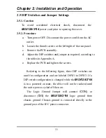
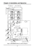
Page 15: ...P switches and jumper as required according to the tables in Appendix A e Replace the PCB and tighten the screws Referring to the following figure three DIP switches are used for configuration and are labeled DSW1 to DSW3 If a DIP switch configuration is changed while the MUX128 2 64 is in a powered on state the effect will not be realized until the unit is power cycled off then on The Logic Groun...

Page 16: ...Chapter 2 Installation and Operation 12 Figure 2 2 MUX128 2 64 Printed Circuit Board Diagram CH 128 Data Port G 703 64K x2 Loop Back Test Sws Indicator LEDs DSW1 DSW2 DSW3 Logic Ground Jumper ...

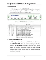
Page 17: ...ormally should be lit during operation Ta yellow Flashes when G 703 A channel transmits data Ra yellow Flashes when G 703 A channel receives data Tb yellow Flashes when G 703 B channel transmits data Rb yellow Flashes when G 703 B channel receives data Err red Indicates error in BERT or slip in A B channel delay Test red Lights when any push button switch is selected Table 2 1 Indicator LED descri...

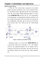
Page 18: ...ed its internal pattern generator and tester will be activated and its signal will be received by the local unit In this configuration both units and the lines are tested Both units will have their Test LEDs lit and Err LEDs should be off Figure 2 4 Back to back BERT testing Referring to figure 2 5 if the remote MUX128 2 64 unit is placed into loop back by placing its Loc ana loopbk switch in the ...

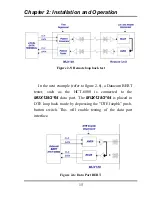
Page 19: ...example refer to figure 2 6 a Datacom BERT tester such as the HCT 6000 is connected to the MUX128 2 64 data port The MUX128 2 64 is placed in DTE loop back mode by depressing the DTE loopbk push button switch This will enable testing of the data port interface Figure 2 6 Data Port BERT ...

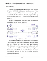
Page 20: ...y function In order to perform auto delay there must be someone at each end of the link refer to figure 2 7 Figure 2 7 Null Delay Feature At the local and remote sites depress the Test switches Then depress the Auto Delay switches on each unit When the Err LEDs go out release the Auto Delay switches The delay both ways has been calculated and saved in each unit Now release the Test switches The de...

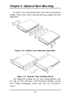
Page 21: ...ndem full space In either situation one standard rack unit space is required Each rack mount kit provides all the necessary hardware for a complete installation Figure 3 1 Rack Mount Installation ETU01 SS In single unit installations the unit may be placed in the left or right side position simply by reversing the rack mounting ears The kit includes one 1 short and one 1 long rack adapter four 4 3...

Page 22: ...efer to the following drawing examples for this application Figure 3 2 Tandem Units Mounting Exploded Figure 3 3 Tandem Units Mounting Detail The tandem kit includes two 2 rack mount adapters one 1 each of inner and outer central mounting adapters twenty 20 3x8mm self tapping screws and four 4 12 24x0 5 screws ...

Page 23: ...very TX timing from data port ON OFF RX and TX timing both from recovery OFF ON RX and TX timing both from data port 1 2 ON ON RX and TX timing both from internal oscillator OFF Recovery timing source Channel A 3 ON Recovery timing source Channel B 4 Reserved 5 Reserved 6 Reserved 7 Reserved 8 Reserved note Factory setting ...

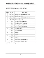
Page 24: ... ON Data port type RS 232 SYNC ONLY 1 2 ON ON Data port type V 36 OFF RX clock polarity NORMAL 3 ON RX clock polarity INVERTED OFF TX clock polarity NORMAL 4 ON TX clock polarity INVERTED OFF CTS Always ON 5 ON CTS Follow RTS OFF Reserved 6 ON Reserved OFF Reserved 7 ON Reserved OFF Front panel switches DISABLE 8 ON Front panel switches ENABLE note Factory setting ...

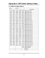
Page 25: ...le 12 ON OFF ON ON OFF Delay clock cycle 13 OFF ON ON ON OFF Delay clock cycle 14 ON ON ON ON OFF Delay clock cycle 15 OFF OFF OFF OFF ON Delay clock cycle 16 ON OFF OFF OFF ON Delay clock cycle 17 OFF ON OFF OFF ON Delay clock cycle 18 ON ON OFF OFF ON Delay clock cycle 19 OFF OFF ON OFF ON Delay clock cycle 20 ON OFF ON OFF ON Delay clock cycle 21 OFF ON ON OFF ON Delay clock cycle 22 ON ON ON O...

Page 26: ...Appendix A DIP Switch Setting Tables 22 This page left blank intentionally ...

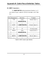
Page 27: ...a 9 pin female D type connector wired in accordance with Table B 1 Pin Designation Direction Function 1 TTIP From MUX128 2 64 Transmit data 2 3 RTIP To MUX128 2 64 Receive data 4 5 FG Frame ground 6 TRING From MUX128 2 64 Transmit data 7 8 RRING To MUX128 2 64 Receive data 9 Table B 1 DB 9 connector pin allocation ...

Page 28: ... output of the MUX128 2 64 2 64K receiver RTS 4 To MUX128 2 64 Supply an ON signal to the MUX128 2 64 2 64k when data transmission is desired CTS 5 From MUX128 2 64 Constantly ON or follow RTS by DIP SW setting DSR 6 From MUX128 2 64 Constantly ON Except during test loops DTR 20 To MUX128 2 64 Not used DCD 8 From MUX128 2 64 Constantly ON ETC 24 To MUX128 2 64 A transmitted data rate clock input f...

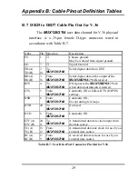
Page 29: ... 2 64K receiver RTS A RTS B 4 19 To MUX128 2 64 ON signal to the MUX128 2 64 2 64k when data transmission is desired CTS A CTS B 5 13 From MUX128 2 64 Constantly ON or follow RTS DIP SW setting DSR A DSR B 6 22 From MUX128 2 64 Constantly ON Except during test loops DTR A DTR B 20 23 To MUX128 2 64 Not used DCD A DCD B 8 10 From MUX128 2 64 Constantly ON ETC A ETC B 24 11 To MUX128 2 64 A transmit...

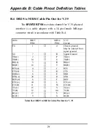
Page 30: ... in accordance with Table B 4 Abbr DB25 PIN MB34 PIN V 35 Circuit FG 1 A Chassis ground May be isolated from signal ground SG 7 B Signal Ground TD A TD B 2 14 P S TD A TD B RD A RD B 3 16 R T RD A RD B RTS A 4 C RTS CTS A 5 D CTS DSR A 6 E DSR DTR A 20 H DTR DCD A 8 F DCD ETC A ETC B 24 11 U W ETC A ETC B TC A TC B 15 12 Y AA TC A TC B RC A RC B 17 9 V X RC A RC B Table B 4 DB25 to MB34 Cable Pin ...

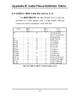
Page 31: ...Abbr DB25 PIN DB15 PIN X 21 Circuit FG 1 1 Chassis ground May be isolated from signal ground SG 7 8 Signal Ground TD A TD B 2 14 2 9 Transmit A Transmit B RD A RD B 3 16 4 11 Receive A Receive B RTS A RTS B 4 19 3 10 Control A Control B DCD A DCD B 8 10 5 12 Indication A Indication B ETC A ETC B 24 11 7 14 External Timing A External Timing B RC A RC B 17 9 6 13 Signal Timing A Signal Timing B Tabl...

Page 32: ...PIN RS 449 Circuit FG 1 1 Chassis ground May be isolated from signal ground SG 7 19 20 37 SG RC SC TD A TD B 2 14 4 22 SD A SD B RD A RD B 3 16 6 24 RD A RD B RTS A RTS B 4 19 7 25 RS A RS B CTS A CTS B 5 13 9 27 CS A CS B DSR A DSR B 6 22 11 29 DM A DM B DTR A DTR B 20 23 12 30 TR A TR B DCD A DCD B 8 10 13 31 RR A RR B ETC A ETC B 24 11 17 35 TT A TT B TC A TC B 15 12 5 23 ST A ST B RC A RC B 17...

Page 33: ... the MUX128 2 64 2 64K receiver RTS 4 To MUX128 2 64 ON signal to the MUX128 2 64 2 64k when data transmission is desired CTS 5 From MUX128 2 64 Constantly ON or follow RTS DIP SW setting DSR 6 From MUX128 2 64 Constantly ON Except during test loops DTR 20 To MUX128 2 64 Not used DCD 8 From MUX128 2 64 Constantly ON ETC A ETC B 24 11 To MUX128 2 64 A transmitted data rate clock input from the data...

Page 34: ......

Page 35: ......
Page 36: ...CTC Union Technologies Co Ltd Far Eastern Vienna Building Neihu Technology Park 8F No 60 ZhouZi St Neihu Taipei Taiwan Phone 886 2 2659 1021 Fax 886 2 2799 1355 E mail info ctcu com http www ctcu com ...

Reviews: