


CHAMP-AV8 (VPX6-462) H
ARDWARE
U
SER
’
S
M
ANUAL
C
URTISS
-W
RIGHT
A-44
P
ROPRIETARY
826448 V
ERSION
5 M
ARCH
2015
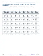
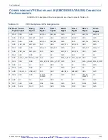
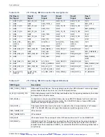
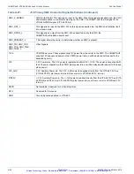
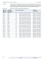
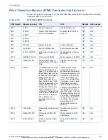
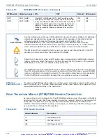
XMC_F_NVMRO
XMC Write Prohibit. This signal is an input to the XMC. When this signal is asserted high, the XMC
shall disable writes to non-volatile memory on the XMC. The CHAMP-AV8 ties this signal to the
VITA 46 NVMRO signal (VITA 46 P0-A4).
XMC_RST_L
This signal is an input to the XMC. When this signal is asserted low, the XMC shall initialize itself
into a known state.
XMC_RSTIN_L
This signal is an output from the XMC. When asserted low by the XMC, the
CHAMP-AV8 will initiate a board reset.
XMC_PRESENT_L
This signal allows the carrier to determine whether an XMC is present.
XMC_TDI, XMC_TDO,
XMC_TCK, XMC_TMS,
XMC_TRST_L
JTAG Signals
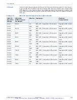
12V0
VPWR Power pins. These signals carry12V power from the carrier to the XMC. The CHAMP-AV8
supplies 12V sequenced power on the VPWR (power turn-on will be delayed with respect to the
backplane power).
3V3
3.3 V Power pins. The 3.3V power is regulated to within 3.3V +/-0.3V. The power is sequenced with
the 3V3 power supplied on the VPWR pins (power turn-on will be delayed with respect to the back-
plane power).
3V3_AUX
3.3 V Auxiliary Power pin. The 3.3V_AUX power is supplied directly from the VITA 46 3.3V Aux
(VITA 46 P0-D5) pin (power turn-on will occur prior to VPWR and 3.3V turn-on).
P/N12V
+/-12 V Auxiliary Power pin. The +/-12V power is supplied directly from the VITA 46 12V Aux (VITA
46 P0-D6) and N12V Aux (VITA 46 P0-D6) pins (power turn-on will occur prior to VPWR and 3.3V
turn-on).
RSVD
Not available- Reserved for Curtiss-Wright use
RFU
Reserved for future use
GND
Ground signals as defined in VITA 42.0.
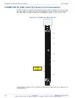
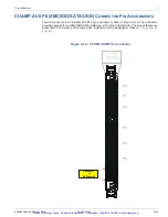
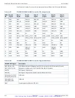
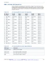
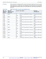
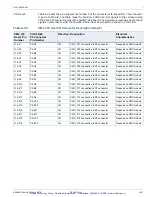
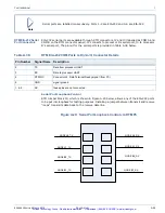
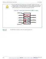
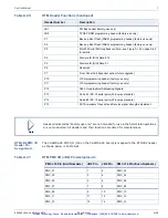
Table A.27:
J15 Primary XMC Connector Signal Definitions (Continued)
Artisan Technology Group - Quality Instrumentation ... Guaranteed | (888) 88-SOURCE | www.artisantg.com