


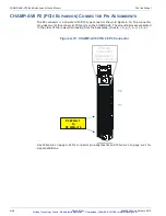


CHAMP-AV8 (VPX6-462) H
ARDWARE
U
SER
’
S
M
ANUAL
C
URTISS
-W
RIGHT
A-8
P
ROPRIETARY
826448 V
ERSION
5 M
ARCH
2015
CHAMP-AV8 I/O M
APPING
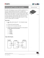
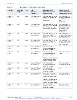
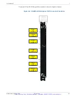
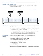
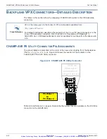
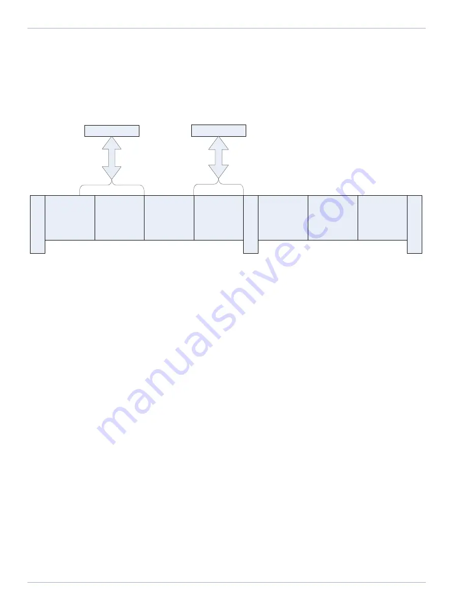
With reference to Figure A.5, the I/O mapping of the various CHAMP-AV8 connectors is
summarized in the following sections.
Figure A.5: I/O Mapping to the CHAMP-AV8 VITA 46 Connectors
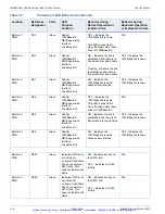
XMC I/O Mapping
The CHAMP-AV8 incorporates one XMC site that populates both the PMC (J14) and the XMC
(J16) I/O connectors.
• The XMC J14 connector (PMC I/O) is mapped to the VITA 46 P3 connector according to
VITA 46.9 P64s pattern. See “Corresponding VPX Backplane J2 (PCIe Expansion) Con-
nector Pin Assignments” on page A-22 for details.
• The XMC J16 connector (XMC I/O) is mapped to the VITA 46 P5 and P6 connectors
according to VITA 46.9, P5w3P6-X38s+X8d+X12d pattern. See “CHAMP-AV8 P5 (XMC
User I/O) Connector Pin Assignments” on page A-30 and “CHAMP-AV8 P6
(XMC/DIO/SATA/USB) Connector Pin Assignments” on page A-33 for details.
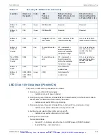
VITA 46 P0 Utility
Connector
The P0 connector on the CHAMP-AV8 supports the following functions/interfaces:
• Power and Ground (BP12V, 3V3AUX, 12AUX, N12AUX, GND) signals
• Geographical Addressing (GA_L[4:0] and GAP_L) signals
• Differential Reference Clock (REF_CLK_P/N) signals
• System Reset (SYSRST_L) signal
• JTAG (TCLK, TDO, TDI, TMS, TRST_L) signals
• AUX_CLK_P/N signals
• No Connect (NC) signals
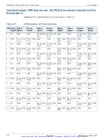
See “CHAMP-AV8 P0 Utility Connector Pin Assignments” on page A-14 for additional details.
Key
P6
P5
P2
P4
Key
P1
P0
Key
J14
P6
4S
J16
X
3
8s
+
X
8
d+
X
12
d
P3
Artisan Technology Group - Quality Instrumentation ... Guaranteed | (888) 88-SOURCE | www.artisantg.com