

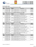


CY7C0837AV, CY7C0830AV
CY7C0831AV, CY7C0832AV
CY7C0832BV, CY7C0833AV
Document #: 38-06059 Rev. *S
Page 24 of 28
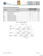
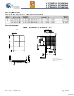
Ordering Information
512K
×
18 (9M) 3.3V Synchronous CY7C0833AV Dual-Port SRAM
Speed
(MHz)
Ordering Code
Package
Diagram
Package Type
Operating
Range
133
CY7C0833AV-133BBC
51-85141 144-Ball Grid Array (13 x 13 x 1.6 mm) with 1 mm pitch
Commercial
CY7C0833AV-133BBI
51-85141 144-Ball Grid Array (13 x 13 x 1.6 mm) with 1 mm pitch
Industrial
100
CY7C0833AV-100BBC
51-85141 144-Ball Grid Array (13 x 13 x 1.6 mm) with 1 mm pitch
Commercial
CY7C0833AV-100BBI
51-85141 144-Ball Grid Array (13 x 13 x 1.6 mm) with 1 mm pitch
Industrial
256K
×
18 (4M) 3.3V Synchronous CY7C0832AV/CY7C0832BV Dual-Port SRAM
Speed
(MHz)
Ordering Code
Package
Diagram
Package Type
Operating
Range
167
CY7C0832AV-167BBC
51-85141 144-Ball Grid Array (13 x 13 x 1.6 mm) with 1 mm pitch
Commercial
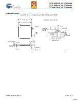
CY7C0832AV-167AC
51-85100 120-Pin Thin Quad Flat Pack (14 x 14 x 1.4 mm)
CY7C0832AV-167AXC
120-Pin Thin Quad Flat Pack (14 x 14 x 1.4 mm) (Pb-Free)
133
CY7C0832AV-133BBC
51-85141 144-Ball Grid Array (13 x 13 x 1.6 mm) with 1 mm pitch
Commercial
CY7C0832AV-133AC
51-85100 120-Pin Thin Quad Flat Pack (14 x 14 x 1.4 mm)
CY7C0832AV-133AXC
120-Pin Thin Quad Flat Pack (14 x 14 x 1.4 mm) (Pb-Free)
CY7C0832AV-133BBI
51-85141 144-Ball Grid Array (13 x 13 x 1.6 mm) with 1 mm pitch
Industrial
CY7C0832BV-133AI
51-85100 120-Pin Thin Quad Flat Pack (14 x 14 x 1.4 mm)
CY7C0832AV-133AXI
120-Pin Thin Quad Flat Pack (14 x 14 x 1.4 mm) (Pb-Free)
128K
×
18 (2M) 3.3V Synchronous CY7C0831AV Dual-Port SRAM
Speed
(MHz)
Ordering Code
Package
Diagram
Package Type
Operating
Range
167
CY7C0831AV-167BBC
51-85141 144-Ball Grid Array (13 x 13 x 1.6 mm) with 1 mm pitch
Commercial
CY7C0831AV-167AC
51-85100 120-Pin Thin Quad Flat Pack (14 x 14 x 1.4 mm)
CY7C0831AV-167AXC
120-Pin Thin Quad Flat Pack (14 x 14 x 1.4 mm) (Pb-Free)
133
CY7C0831AV-133BBC
51-85141 144-Ball Grid Array (13 x 13 x 1.6 mm) with 1 mm pitch
Commercial
CY7C0831AV-133BBXC
144-Ball Grid Array (13 x 13 x 1.6 mm) with 1 mm pitch (Pb-Free)
CY7C0831AV-133AC
51-85100 120-Pin Thin Quad Flat Pack (14 x 14 x 1.4 mm)
CY7C0831AV-133AXC
120-Pin Thin Quad Flat Pack (14 x 14 x 1.4 mm) (Pb-Free)
CY7C0831AV-133BBI
51-85141 144-Ball Grid Array (13 x 13 x 1.6 mm) with 1 mm pitch
Industrial
CY7C0831AV-133BBXI
144-Ball Grid Array (13 x 13 x 1.6 mm) with 1 mm pitch (Pb-Free)
CY7C0831AV-133AI
51-85100 120-Pin Thin Quad Flat Pack (14 x 14 x 1.4 mm)
CY7C0831AV-133AXI
120-Pin Thin Quad Flat Pack (14 x 14 x 1.4 mm) (Pb-Free)
64K
×
18 (1M) 3.3V Synchronous CY7C0830AV Dual-Port SRAM
Speed
(MHz)
Ordering Code
Package
Diagram
Package Type
Operating
Range
167
CY7C0830AV-167BBC
51-85141 144-Ball Grid Array (13 x 13 x 1.6 mm) with 1 mm pitch
Commercial
CY7C0830AV-167AC
51-85100 120-Pin Thin Quad Flat Pack (14 x 14 x 1.4 mm)
133
CY7C0830AV-133BBC
51-85141 144-Ball Grid Array (13 x 13 x 1.6 mm) with 1 mm pitch
Commercial
CY7C0830AV-133AC
51-85100 120-Pin Thin Quad Flat Pack (14 x 14 x 1.4 mm)
CY7C0830AV-133BBI
51-85141 144-Ball Grid Array (13 x 13 x 1.6 mm) with 1 mm pitch
Industrial
CY7C0830AV-133AI
51-85100 120-Pin Thin Quad Flat Pack (14 x 14 x 1.4 mm)
[+] Feedback


