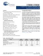
CY7C0850AV, CY7C0851AV
CY7C0852AV, CY7C0853AV
Document #: 38-06070 Rev. *H
Page 13 of 32
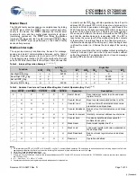
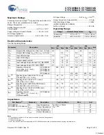
Maximum Ratings
Exceeding maximum ratings
[15]
may impair the useful life of the
device. These user guidelines are not tested.
Storage Temperature................................ –65
°
C to + 150
°
C
Ambient Temperature with
Power Applied ........................................... –55
°
C to + 125
°
C
Supply Voltage to Ground Potential...............–0.5V to + 4.6V
DC Voltage Applied to
Outputs in High-Z State ......................... –0.5V to V
DD
+ 0.5V
DC Input Voltage .............................. –0.5V to V
DD
+ 0.5V
[16]
Output Current into Outputs (LOW)............................. 20 mA
Static Discharge Voltage........................................... > 2000V
(JEDEC JESD22-A114-2000B)
Latch-up Current .................................................... > 200 mA
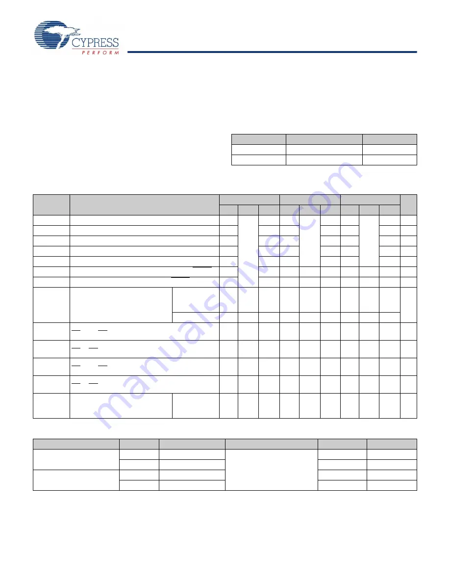
Operating Range
Range
Ambient Temperature
V
DD
Commercial
0
°
C to +70
°
C
3.3V ± 165 mV
Industrial
–40
°
C to +85
°
C
3.3V ± 165 mV
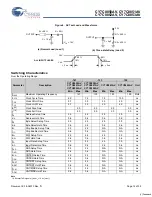
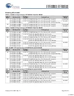
Electrical Characteristics
Over the Operating Range
Parameter
Description
-167
-133
-100
Unit
Min
Typ.
Max
Min
Typ.
Max
Min Typ.
Max
V
OH
Output HIGH Voltage (V
DD
= Min., I
OH
= –4.0 mA)
2.4
2.4
2.4
V
V
OL
Output LOW Voltage (V
DD
= Min., I
OL
= +4.0 mA)
0.4
0.4
0.4
V
V
IH
Input HIGH Voltage
2.0
2.0
2.0
V
V
IL
Input LOW Voltage
0.8
0.8
0.8
V
I
OZ
Output Leakage Current
–10
10
–10
10
–10
10
μ
A
I
IX1
Input Leakage Current Except TDI, TMS, MRST
–10
10
–10
10
–10
10
μ
A
I
IX2
Input Leakage Current TDI, TMS, MRST
–0.1
1.0
–0.1
1.0
–0.1
1.0
mA
I
CC
Operating Current for
(V
DD
= Max.,I
OUT
= 0 mA),
Outputs Disabled
CY7C0850AV
CY7C0851AV
CY7C0852AV
225
300
225
300
mA
CY7C0853AV
270
400
200
310
I
SB1
[18]
Standby Current (Both Ports TTL Level)
CE
L
and CE
R
≥
V
IH
, f = f
MAX
90
115
90
115
90
115
mA
I
SB2
[18]
Standby Current (One Port TTL Level)
CE
L
| CE
R
≥
V
IH
, f = f
MAX
160
210
160
210
160
210
mA
I
SB3
[18]
Standby Current (Both Ports CMOS Level)
CE
L
and CE
R
≥
V
DD
– 0.2V, f = 0
55
75
55
75
55
75
mA
I
SB4
[18]
Standby Current (One Port CMOS Level)
CE
L
| CE
R
≥
V
IH
, f = f
MAX
160
210
160
210
160
210
mA
I
SB5
Operating Current
(V
DD
= Max, I
OUT
= 0 mA, f = 0)
Outputs Disabled
CY7C0853AV
70
100
70
100
mA
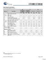
Capacitance
Part Number
[17]
Parameter
Description
Test Conditions
Max
Unit
CY7C0850AV,
CY7C0851AV, CY7C0852AV
C
IN
Input Capacitance
T
A
= 25
°
C, f = 1 MHz,
V
DD
= 3.3V
13
pF
C
OUT
Output Capacitance
10
pF
CY7C0853AV
C
IN
Input Capacitance
22
pF
C
OUT
Output Capacitance
20
pF
Notes
15. The voltage on any input or I/O pin can not exceed the power pin during power up.
16. Pulse width < 20 ns.
17. C
OUT
also references C
I/O
.
18. I
SB1
, I
SB2
, I
SB3
and I
SB4
are not applicable for CY7C0853AV because it can not be powered down by using chip enable pins.
[+] Feedback


