background image

CYD01S36V

CYD02S36V/36VA/CYD04S36V

CYD09S36V/CYD18S36V

Document Number: 38-06076 Rev. *G

Page 24 of 28

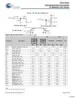
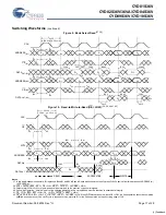
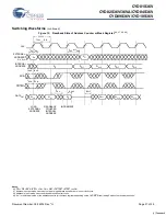
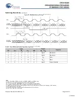
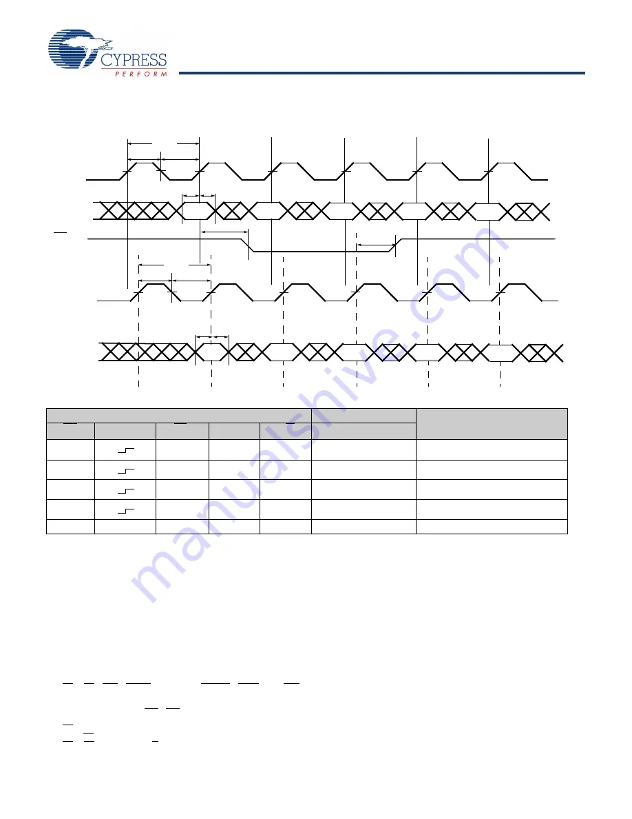
Figure 18.  MailBox Interrupt Timing

[57, 58, 59, 60, 61]
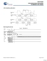
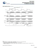
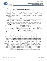
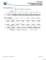
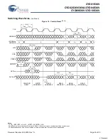
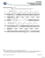
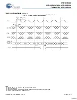
Switching Waveforms 

 (continued)

t

CH2

t

CL2

t

CYC2

CLK

L

t

CH2

t

CL2

t

CYC2

CLK

R

7FFFF

t

SA

t

HA

A

n+3

A

n

A

n+1

A

n+2

L_PORT

ADDRESS

A

m

A

m+4

A

m+1

7FFFF

A

m+3

R_PORT

ADDRESS

INT

R

t

SA

t

HA

t

SINT

t

RINT

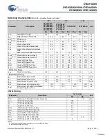
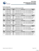
Table 7.  Read/Write and Enable Operation


(Any Port)

[1, 18, 62, 63, 64]

Inputs

Outputs

Operation

OE

CLK

CE

0

CE

1

R/W

DQ

0

 – 

DQ

35

X

H

X

X

High-Z

Deselected

X

X

L

X

High-Z

Deselected

X

L

H

L

D

IN

Write

L

L

H

H

D

OUT

Read

H

X

L

H

X

High-Z

Outputs Disabled

Notes

57. CE

0

 = OE = ADS = CNTEN = LOW; CE

1

 = CNTRST = MRST = CNT/MSK = HIGH.

58. Address “7FFFF” is the mailbox location for R_Port of the 9-Mbit device.
59. L_Port is configured for Write operation, and R_Port is configured for Read operation.
60. At least one byte enable (BE0 – BE3) is required to be active during interrupt operations.
61. Interrupt flag is set with respect to the rising edge of the Write clock, and is reset with respect to the rising edge of the Read clock.
62. OE is an asynchronous input signal.
63. When CE changes state, deselection and Read happen after one cycle of latency.
64. CE

0

 = OE = LOW; CE

1

 = R/W = HIGH.

[+] Feedback 

Summary of Contents for FLEx36 CYD01S36V

Page 1: ...dress and data lines allow for minimal setup and hold time During a Read operation data is registered for decreased cycle time Each port contains a burst counter on the input address register After externally loading the counter with the initial address the counter increments the address internally more details to follow The internal Write pulse width is independent of the duration of the R W inpu...

Page 2: ... CL WRPL A 18 0 R CNT MSKR ADSR CNTENR CNTRSTR RETR CNTINTR CR WRPR CONFIG Block CONFIG Block IO Control IO Control Dual Ported Array Address Counter Logic Address Counter Logic INTL TRST TMS TDI TDO TCK JTAG MRST READYR LowSPDR READYL LowSPDL RESET LOGIC INTR BUSYL BUSYR Mailboxes Arbitration Logic Note 1 18 Mbit device has 19 address bits 9 Mbit device has 18 address bits 4 Mbit device has 17 ad...

Page 3: ...L VDDIOL VDDIOL VCORE VCORE VDDIO R VDDIO R VDDIO R REVR 2 4 R WR A17R 8 A16R 7 N A18L 9 A19L 2 5 CNT M SKL 10 VREFL 2 4 PortST D0L 2 4 READY L 2 5 REVL 2 3 VTTL VTTL REVR 2 3 READY R 2 5 PortST D0R 2 4 VREFR 2 4 CNT M SKR 10 A19R 2 5 A18R 9 P DQ16L DQ17L CNTEN L 11 CNTRS TL 10 NC 2 5 NC 2 5 TCK TMS TDO TDI NC 2 5 NC 2 5 CNTRS TR 10 CNTEN R 11 DQ17R DQ16R R DQ15L DQ13L DQ11L DQ9L DQ7L DQ5L DQ3L DQ...

Page 4: ...s ready for normal operation CNT MSKL 10 CNT MSKR 10 Port Counter Mask Select Input Counter control input ADSL 11 ADSR 11 Port Counter Address Load Strobe Input Counter control input CNTENL 11 CNTENR 11 Port Counter Enable Input Counter control input CNTRSTL 10 CNTRSTR 10 Port Counter Reset Input Counter control input CNTINTL 12 CNTINTR 12 Port Counter Interrupt Output This pin is asserted LOW whe...

Page 5: ... Counter Reset operations by preventing the corresponding bits of the counter register from changing It also affects the counter interrupt output CNTINT The mask register is changed only by the Mask Load and Mask Reset operations and by the MRST The mask register defines the counting range of the counter register It divides the counter register into two regions zero or more 0s in the most signific...

Page 6: ... Reset followed by a Counter Reset resets the counter and mirror registers to 00000 as does master reset MRST Counter Load Operation The address counter and mirror registers are both loaded with the address value presented at the address lines Table 3 Address Counter and Counter Mask Register Control Operation Any Port 18 20 CLK MRST CNT MSK CNTRST ADS CNTEN Operation Description X L X X X X Maste...

Page 7: ...d by Counter Reset Counter Load Mask Reset and Mask Load operations and by MRST Counter Readback Operation The internal value of the counter register can be read out on the address lines Readback is pipelined the address is valid tCA2 after the next rising edge of the port s clock If address readback occurs while the port is enabled CE0 LOW and CE1 HIGH the data lines DQs are three stated Figure 2...

Page 8: ...rap 1 0 Increment Logic 1 0 1 2 1 0 Wrap Detect From Mask From Counter To Counter Bit 0 Wrap Figure 2 Counter Mask and Mirror Logic Block Diagram 1 17 17 17 17 17 1 0 Load Increment CNT MSK CNTEN ADS CNTRST CLK Decode Logic Bidirectional Address Lines Mask Register Counter Address Register From Address Lines To Readback and Address Decode 17 17 MRST Feedback ...

Page 9: ... hierar chical approach as shown in Figure 4 on page 10 and Figure 5 on page 10 TMS and TCK are connected in parallel to each DIE to drive all 2 or 4 TAP controllers in unison In many cases each DIE is supplied with the same instruction In other cases it might be useful to supply different instructions to each DIE One example would be testing the device ID of one DIE while bypassing the rest Each ...

Page 10: ...er 31 28 0h Reserved for version number Cypress Device ID 27 12 C002h Defines Cypress part number for CYD04S36V CYD09S36V and CYD18S36V C001h Defines Cypress part number for CYD02S36V 36VA C092h Defines Cypress part number for CYD01S36V Cypress JEDEC ID 11 1 034h Allows unique identification of the DP family device vendor ID Register Presence 0 1 Indicates the presence of an ID register Table 5 Sc...

Page 11: ...E 1011 Loads the IDR with the vendor ID code and places the register between TDI and TDO HIGHZ 0111 Places BYR between TDI and TDO Forces all device output drivers to a High Z state CLAMP 0100 Controls boundary to 1 0 Places BYR between TDI and TDO SAMPLE PRELOAD 1000 Captures the input output ring contents Places BSR between TDI and TDO NBSRST 1100 Resets the non boundary scan logic Places BYR be...

Page 12: ...ltage VDD Min IOH 4 0 mA 2 4 2 4 2 4 V VOL Output LOW Voltage VDD Min IOL 4 0 mA 0 4 0 4 0 4 V VIH Input HIGH Voltage 2 0 2 0 2 0 V VIL Input LOW Voltage 0 8 0 8 0 8 V IOZ Output Leakage Current 10 10 10 10 10 10 μA IIX1 Input Leakage Current Except TDI TMS MRST 10 10 10 10 10 10 μA IIX2 Input Leakage Current TDI TMS MRST 1 0 0 1 1 0 0 1 1 0 0 1 mA ICC Operating Current for VDD Max IOUT 0 mA Outpu...

Page 13: ...ddress Hold Time 0 6 0 6 1 0 1 0 ns tSB Byte Select Setup Time 2 3 2 5 2 2 2 7 ns tHB Byte Select Hold Time 0 6 0 6 1 0 1 0 ns tSC Chip Enable Setup Time 2 3 2 5 NA NA ns tHC Chip Enable Hold Time 0 6 0 6 NA NA ns tSW R W Setup Time 2 3 2 5 2 2 2 7 ns tHW R W Hold Time 0 6 0 6 1 0 1 0 ns tSD Input Data Setup Time 2 3 2 5 2 2 2 7 ns tHD Input Data Hold Time 0 6 0 6 1 0 1 0 ns tSAD ADS Setup Time 2 ...

Page 14: ... 7 8 0 ns Master Reset Timing tRS Master Reset Pulse Width 5 0 5 0 5 0 5 0 cycles tRS Master Reset Setup Time 6 0 6 0 6 0 8 5 ns tRSR Master Reset Recovery Time 5 0 5 0 5 0 5 0 cycles tRSF Master Reset to Outputs Inactive 10 0 10 0 10 0 10 0 ns tRSINT Master Reset to Counter and Mailbox Interrupt Flag Reset Time 10 0 10 0 NA NA ns Switching Characteristics Over the Operating Range continued Parame...

Page 15: ...JTAG Switching Waveform Test Clock Test Mode Select TCK TMS Test Data In TDI Test Data Out TDO tTCYC tTMSH tTL tTH tTMSS tTDIS tTDIH tTDOX tTDOV Switching Waveforms Figure 7 Master Reset MRST tRSR tRS INACTIVE ACTIVE TMS TDO INT CNTINT tRSF tRSS ALL ADDRESS DATA LINES ALL OTHER INPUTS tRSINT Feedback ...

Page 16: ...T MSK HIGH 35 The output is disabled high impedance state by CE VIH following the next rising edge of the clock 36 Addresses do not have to be accessed sequentially since ADS CNTEN VIL with CNT MSK VIH constantly loads the address on the rising edge of the CLK Numbers are for reference only Switching Waveforms continued tCH2 tCL2 tCYC2 tSC tHC tSW tHW tSA tHA An An 1 CLK CE R W ADDRESS DATAOUT OE ...

Page 17: ...e rewritten to ensure data integrity 41 CE0 OE BE0 BE3 LOW CE1 R W CNTRST MRST HIGH 42 CE0 BE0 BE3 R W LOW CE1 CNTRST MRST CNT MSK HIGH When R W first switches low since OE LOW the Write operation cannot be completed labelled as no operation One clock cycle is required to three state the IO for the Write operation on the next rising edge of CLK Switching Waveforms continued Q3 Q1 Q0 Q2 A0 A1 A2 A3...

Page 18: ...itching Waveforms continued tCYC2 tCL2 tCH2 tHC tSC tHW tSW tHA tSA An An 1 An 2 An 3 An 4 An 5 tHW tSW tSD tHD Dn 2 tCD2 tOHZ READ READ WRITE Dn 3 Qn CLK CE R W ADDRESS DATAIN DATAOUT OE Qn 4 tCD2 tSA tHA tCH2 tCL2 tCYC2 CLK ADDRESS An COUNTER HOLD READ WITH COUNTER tSAD tHAD tSCN tHCN tSAD tHAD tSCN tHCN Qx 1 Qx Qn Qn 1 Qn 2 Qn 3 tDC tCD2 READ WITH COUNTER READ EXTERNAL ADDRESS ADS CNTEN DATAOUT...

Page 19: ...3 Write with Address Counter Advance 42 Switching Waveforms continued tCH2 tCL2 tCYC2 An An 1 An 2 An 3 An 4 Dn 1 Dn 1 Dn 2 Dn 3 Dn 4 An Dn tSAD tHAD tSCN tHCN tSD tHD WRITE EXTERNAL WRITE WITH COUNTER ADDRESS WRITE WITH COUNTER WRITE COUNTER HOLD CLK ADDRESS INTERNAL DATAIN ADDRESS tSA tHA CNTEN ADS Feedback ...

Page 20: ...y be coincidental with the counter reset 45 Retransmit happens if the counter remains in increment mode after it wraps to initially loaded value Switching Waveforms continued CLK ADDRESS INTERNAL CNTEN ADS DATAIN ADDRESS CNTRST R W DATAOUT An Am Ap Ax 0 1 An Am Ap Q1 Qn Q0 D0 tCH2 tCL2 tCYC2 tSA tHA tSW tHW tSRST tHRST tSD tHD tCD2 tCD2 tCKLZ 45 RESET ADDRESS 0 COUNTER WRITE READ ADDRESS 0 ADDRESS...

Page 21: ...lock cycle 48 Address in input mode Host can drive address bus after tCKHZ 49 An is the internal value of the address counter or the mask register depending on the CNT MSK level being Read out on the address lines Switching Waveforms continued CNTEN CLK tCH2 tCL2 tCYC2 ADDRESS ADS An Qx 2 Qx 1 Qn tSA tHA tSAD tHAD tSCN tHCN LOAD ADDRESS EXTERNAL tCD2 INTERNAL ADDRESS An 1 An 2 An tCKHZ DATAOUT An ...

Page 22: ... is violated indeterminate data is Read out 52 If tCCS minimum specified value then R_Port Reads the most recent data written by L_Port only 2 tCYC2 tCD2 after the rising edge of R_Port s clock If tCCS minimum specified value then R_Port Reads the most recent data written by L_Port tCYC2 tCD2 after the rising edge of R_Port s clock Switching Waveforms continued tSA tHA tSW tHW tCH2 tCL2 tCYC2 CLKL...

Page 23: ...1 R W CNTRST MRST HIGH 54 CNTINT is always driven 55 CNTINT goes LOW when the unmasked portion of the address counter is incremented to the maximum value 56 The mask register assumed to have the value of 3FFFFh Switching Waveforms continued tCH2 tCL2 tCYC2 CLK 3FFFD 3FFFF INTERNAL ADDRESS Last_Loaded Last_Loaded 1 tHCM COUNTER 3FFFE CNTINT tSCINT tRCINT 3FFFC CNTEN ADS CNT MSK tSCM Feedback ...

Page 24: ...gh Z Deselected X L H L DIN Write L L H H DOUT Read H X L H X High Z Outputs Disabled Notes 57 CE0 OE ADS CNTEN LOW CE1 CNTRST MRST CNT MSK HIGH 58 Address 7FFFF is the mailbox location for R_Port of the 9 Mbit device 59 L_Port is configured for Write operation and R_Port is configured for Read operation 60 At least one byte enable BE0 BE3 is required to be active during interrupt operations 61 In...

Page 25: ...CYD04S36V Dual Port SRAM Speed MHz Ordering Code Package Name Package Type Operating Range 167 CYD04S36V 167BBC BB256 256 ball Grid Array 17 mm 17 mm with 1 0 mm pitch BGA Commercial 133 CYD04S36V 133BBC BB256 256 ball Grid Array 17 mm 17 mm with 1 0 mm pitch BGA Commercial CYD04S36V 133BBI BB256 256 ball Grid Array 17 mm 17 mm with 1 0 mm pitch BGA Industrial 64K 36 2 Mbit 3 3V Synchronous CYD02S...

Page 26: ...A B Ø0 05 M C Ø0 45 0 05 256X CPLD DEVICES 37K 39K 0 25 C 0 70 0 05 C SEATING PLANE 0 15 C 16 15 14 13 12 11 T R P M N L N T R P M L K J F G H E D A C B 16 15 13 14 12 10 11 9 2 8 7 6 5 4 3 1 A B Ø0 50 256X ALL OTHER DEVICES 0 10 0 05 A1 0 36 0 56 A 1 40 MAX 1 70 MAX REFERENCE JEDEC MO 192 15 00 1 00 0 35 A 17 00 0 10 7 50 7 50 15 00 17 00 0 10 1 00 A1 0 05 0 10 51 85108 F Figure 19 256 Ball FBGA ...

Page 27: ...J K PIN 1 CORNER PIN 1 CORNER 0 20 4X Ø0 25 M C A B Ø0 05 M C 0 25 C 0 70 0 05 C SEATING PLANE 0 15 C 0 35 16 15 14 13 12 11 T R P M N L N T R P M L K J F G H E D A C B 16 15 13 14 12 10 11 9 2 8 7 6 5 4 3 1 23 00 0 10 A B 7 50 7 50 15 00 23 00 0 10 1 00 Ø0 50 256X 0 05 0 10 0 10 0 05 1 70 MAX 0 56 JEDEC MO 192 51 85201 A Figure 20 256 ball FBGA 23 mm x 23 mm x 1 7 mm BB256B Feedback ...

Page 28: ...T LIMITED TO THE IMPLIED WARRANTIES OF MERCHANTABILITY AND FITNESS FOR A PARTICULAR PURPOSE Cypress reserves the right to make changes without further notice to the materials described herein Cypress does not assume any liability arising out of the application or use of any product or circuit described herein Cypress does not authorize its products for use as critical components in life support sy...

Reviews: