background image

PRELIMINARY

CY14B102L, CY14B102N

Document #: 001-45754 Rev. *B

Page 10 of 24

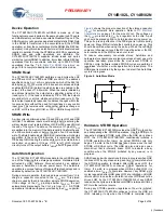
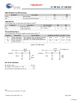
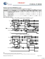
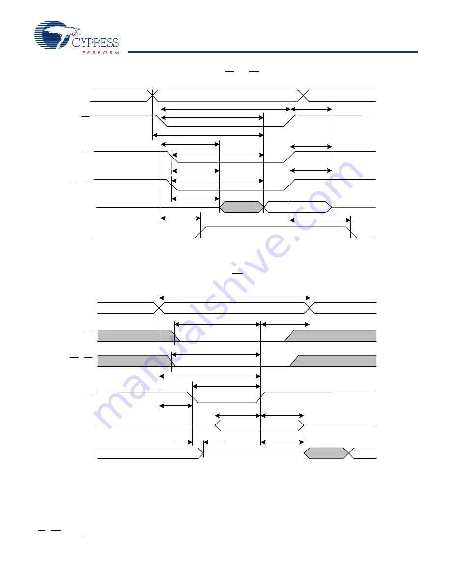
Figure 7.  SRAM Read Cycle #2: CE and OE Controlled

[3, 15, 19]

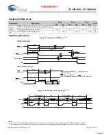
Figure 8.  SRAM Write Cycle #1: WE Controlled

[3, 18, 19, 20]


$GGUHVV9DOLG

$GGUHVV

'DWD2XWSXW

2XWSXW'DWD9DOLG

6WDQGE\

$FWLYH

+LJK,PSHGDQFH

&(

2(

%+(%/(

,

&&

W

+=&(

W

5&

W

$&(

W

$$

W

/=&(

W

'2(

W

/=2(

W

'%(

W

/=%(

W

38

W

3'

W

+=%(

W

+=2(

'DWD2XWSXW

'DWD,QSXW

,QSXW'DWD9DOLG

+LJK,PSHGDQFH

$GGUHVV9DOLG

$GGUHVV

3UHYLRXV'DWD

W

:&

W

6&(

W

+$

W

%:

W

$:

W

3:(

W

6$

W

6'

W

+'

W

+=:(

W

/=:(

:(

%+(%/(

&(

Notes

20. CE or WE must be >V

IH

 during address transitions.

[+] Feedback 

Summary of Contents for Perform CY14B102L

Page 1: ... a nonvolatile element in each memory cell The memory is organized as 256K bytes of 8 bits each or 128K words of 16 bits each The embedded nonvolatile elements incorporate QuantumTrap technology producing the world s most reliable nonvolatile memory The SRAM provides infinite read and write cycles while independent nonvolatile data resides in the highly reliable QuantumTrap cell Data transfers fro...

Page 2: ... 4 Mbit NC pin not connected to die 5 Address expansion for 8 Mbit NC pin not connected to die 6 Address expansion for 16 Mbit NC pin not connected to die 7 HSB pin is not available in 44 TSOP II x16 package 44 TSOP II x16 44 TSOP II x8 7 NC A8 NC NC VSS DQ6 DQ5 DQ4 VCC A13 DQ3 A12 DQ2 DQ1 DQ0 OE A9 CE NC A0 A1 A2 A3 A4 A5 A6 A11 A7 A14 A15 A16 A17 NC NC 1 2 3 4 5 6 7 8 9 10 11 12 13 14 15 16 17 1...

Page 3: ...ctive LOW Controls DQ15 DQ8 BLE Input Byte Low Enable Active LOW Controls DQ7 DQ0 VSS Ground Ground for the Device Must be connected to the ground of the system VCC Power Supply Power Supply Inputs to the Device HSB 7 Input Output Hardware Store Busy HSB When LOW this output indicates that a hardware store is in progress When pulled LOW external to the chip it initiates a nonvolatile STORE operati...

Page 4: ...ation is a unique feature of QuantumTrap technology and is enabled by default on the CY14B102L CY14B102N During a normal operation the device draws current from VCC to charge a capacitor connected to the VCAP pin This stored charge is used by the chip to perform a single STORE operation If the voltage on the VCC pin drops below VSWITCH the part automatically disconnects the VCAP pin from VCC A STO...

Page 5: ...B will be driven LOW It is important to use read cycles and not write cycles in the sequence although it is not necessary that OE be LOW for a valid sequence After the tSTORE cycle time is fulfilled the SRAM is activated again for the read and write operation Software RECALL Transfer the data from the nonvolatile memory to the SRAM with a software address sequence A software RECALL cycle is initia...

Page 6: ... must be issued to save the AutoStore state through subsequent power down cycles The part comes from the factory with AutoStore enabled Data Protection The CY14B102L CY14B102N protects data from corruption during low voltage conditions by inhibiting all externally initiated STORE and write operations The low voltage condition is detected when VCC VSWITCH If the CY14B102L CY14B102N is in a write mo...

Page 7: ...RC 25 ns tRC 45 ns Values obtained without output loads IOUT 0 mA Automotive 90 75 mA mA ICC2 Average VCC Current during STORE All Inputs Don t Care VCC Max Average current for duration tSTORE 10 mA ICC3 11 AverageVCC Currentat tRC 200 ns 3V 25 C typical All I P cycling at CMOS levels Values obtained without output loads IOUT 0 mA 35 mA ICC4 Average VCAP Current during AutoStore Cycle All Inputs D...

Page 8: ...ut Capacitance TA 25 C f 1 MHz VCC 0 to 3 0V 7 pF COUT Output Capacitance 7 pF Thermal Resistance In the following table the thermal resistance parameters are listed 14 Parameter Description Test Conditions 48 FBGA 44 TSOP II 54 TSOP II Unit ΘJA Thermal Resistance Junction to Ambient Test conditions follow standard test methods and procedures for measuring thermal impedance in accordance with EIA ...

Page 9: ...0 0 0 ns tHZBE Byte Disable to Output Inactive 8 10 15 ns SRAM Write Cycle tWC tWC Write Cycle Time 20 25 45 ns tPWE tWP Write Pulse Width 15 20 30 ns tSCE tCW Chip Enable To End of Write 15 20 30 ns tSD tDW Data Setup to End of Write 8 10 15 ns tHD tDH Data Hold After End of Write 0 0 0 ns tAW tAW Address Setup to End of Write 15 20 30 ns tSA tAS Address Setup to Start of Write 0 0 0 ns tHA tWR A...

Page 10: ...re 8 SRAM Write Cycle 1 WE Controlled 3 18 19 20 GGUHVV 9DOLG GGUHVV DWD 2XWSXW 2XWSXW DWD 9DOLG 6WDQGE FWLYH LJK PSHGDQFH 2 W W5 W W W W 2 W 2 W W W38 W3 W W 2 DWD 2XWSXW DWD QSXW QSXW DWD 9DOLG LJK PSHGDQFH GGUHVV 9DOLG GGUHVV 3UHYLRXV DWD W W6 W W W W3 W6 W6 W W W Notes 20 CE or WE must be VIH during address transitions Feedback ...

Page 11: ...ite Cycle 2 CE Controlled 3 18 19 20 Figure 10 SRAM Write Cycle 3 BHE and BLE Controlled 3 18 19 20 DWD 2XWSXW DWD QSXW QSXW DWD 9DOLG LJK PSHGDQFH GGUHVV 9DOLG GGUHVV W W6 W W6 W6 W W W W3 DWD 2XWSXW DWD QSXW QSXW DWD 9DOLG LJK PSHGDQFH GGUHVV 9DOLG GGUHVV W W6 W W6 W6 W W W W3 Feedback ...

Page 12: ...Waveforms Figure 11 AutoStore or Power Up RECALL 24 96 7 9 6 99 5 6 W6725 W6725 W W W W W 6 W 6 W 5 W 5 6 287 XWRVWRUH 32 5 83 5 5HDG ULWH QKLELWHG 5 32 5 83 5 5HDG ULWH 52 1 287 XWRVWRUH 32 5 83 5 5HDG ULWH 32 5 2 1 XWRVWRUH 1RWH 1RWH 1RWH Notes 21 tHRECALL starts from the time VCC rises above VSWITCH 22 If an SRAM write has not taken place since the last nonvolatile cycle no AutoStore or Hardwar...

Page 13: ...0 ns tHA Address Hold Time 0 0 0 ns tRECALL RECALL Duration 200 200 200 μs Switching Waveforms Figure 12 CE and OE Controlled Software STORE RECALL Cycle 27 Figure 13 Autostore Enable Disable Cycle W5 W5 W6 W W W6 W W W W W W W W6725 W5 W W 6 LJK PSHGDQFH GGUHVV GGUHVV GGUHVV 2 6 6725 RQO 4 7 5 W5 W5 W6 W W W6 W W W W W W W GGUHVV GGUHVV GGUHVV 2 4 7 5 W66 Notes 26 The software sequence is clocked...

Page 14: ...ing 28 29 W3 6 W3 6 W W 6 W W6725 W W 6 ULWH ODWFK VHW ULWH ODWFK QRW VHW 6 1 6 287 4 DWD 2XW 5 6 1 6 287 5 6 SLQ LV GULYHQ KLJK WR 9 RQO E QWHUQDO 65 0 LV GLVDEOHG DV ORQJ DV 6 1 LV GULYHQ ORZ 6 GULYHU LV GLVDEOHG W 6 N2KP UHVLVWRU GGUHVV GGUHVV GGUHVV GGUHVV 6RIW 6HTXHQFH RPPDQG W66 W66 GGUHVV 9 W6 W 6RIW 6HTXHQFH RPPDQG W Notes 28 This is the amount of time it takes to take action on a soft seq...

Page 15: ...n CE WE OE BHE BLE Inputs Outputs 2 Mode Power H X X X X High Z Deselect Power down Standby L X X H H High Z Output Disabled Active L H L L L Data Out DQ0 DQ15 Read Active L H L H L Data Out DQ0 DQ7 DQ8 DQ15 in High Z Read Active L H L L H Data Out DQ8 DQ15 DQ0 DQ7 in High Z Read Active L H H L L High Z Output Disabled Active L H H H L High Z Output Disabled Active L H H L H High Z Output Disabled...

Page 16: ...60 54 pin TSOP II Commercial CY14B102L ZSP20XIT 51 85160 54 pin TSOP II Industrial CY14B102L ZSP20XI 51 85160 54 pin TSOP II CY14B102L ZSP20XAT 51 85160 54 pin TSOP II Automotive CY14B102N ZS20XCT 51 85087 44 pin TSOP II Commercial CY14B102N ZS20XIT 51 85087 44 pin TSOP II Industrial CY14B102N ZS20XI 51 85087 44 pin TSOP II CY14B102N ZS20XAT 51 85087 44 pin TSOP II Automotive CY14B102N BA20XCT 51 ...

Page 17: ...P25XI 51 85160 54 pin TSOP II CY14B102L ZSP25XAT 51 85160 54 pin TSOP II Automotive CY14B102N ZS25XCT 51 85087 44 pin TSOP II Commercial CY14B102N ZS25XIT 51 85087 44 pin TSOP II Industrial CY14B102N ZS25XI 51 85087 44 pin TSOP II CY14B102N ZS25XAT 51 85087 44 pin TSOP II Automotive CY14B102N BA25XCT 51 85128 48 ball FBGA Commercial CY14B102N BA25XIT 51 85128 48 ball FBGA Industrial CY14B102N BA25...

Page 18: ...tive CY14B102N ZS45XCT 51 85087 44 pin TSOP II Commercial CY14B102N ZS45XIT 51 85087 44 pin TSOP II Industrial CY14B102N ZS45XI 51 85087 44 pin TSOP II CY14B102N ZS45XAT 51 85087 44 pin TSOP II Automotive CY14B102N BA45XCT 51 85128 48 ball FBGA Commercial CY14B102N BA45XIT 51 85128 48 ball FBGA Industrial CY14B102N BA45XI 51 85128 48 ball FBGA CY14B102N BA45XAT 51 85128 48 ball FBGA Automotive CY1...

Page 19: ...Std Speed 20 20ns 45 45 ns Data Bus L x8 N x16 Density 102 2 Mb Voltage B 3 0V Cypress CY 14 B 102 L ZS P 20 X C T NVSRAM 14 Auto Store Software Store Hardware Store Temperature C Commercial 0 to 70 C I Industrial 40 to 85 C Pb Free Package BA 48 FBGA ZS TSOP II P 54 Pin Blank 44 Pin A Automotive 40 to 125 C 25 25ns Feedback ...

Page 20: ...0 PLANE SEATING PIN 1 I D 44 1 18 517 0 729 0 800 BSC 0 5 0 400 0 016 0 300 0 012 EJECTOR PIN R G O K E A X S 11 735 0 462 10 058 0 396 10 262 0 404 1 194 0 047 0 991 0 039 0 150 0 0059 0 050 0 0020 0 0315 18 313 0 721 10 058 0 396 10 262 0 404 0 597 0 0235 0 406 0 0160 0 210 0 0083 0 120 0 0047 BASE PLANE 0 10 004 22 23 TOP VIEW BOTTOM VIEW 51 85087 A Feedback ...

Page 21: ...ge Diagrams continued A 1 A1 CORNER 0 75 0 75 Ø0 30 0 05 48X Ø0 25 M C A B Ø0 05 M C B A 0 15 4X 0 21 0 05 1 20 MAX C SEATING PLANE 0 53 0 05 0 25 C 0 15 C A1 CORNER TOP VIEW BOTTOM VIEW 2 3 4 3 75 5 25 B C D E F G H 6 5 4 6 5 2 3 1 D H F G E C B A 6 00 0 10 10 00 0 10 A 10 00 0 10 6 00 0 10 B 1 875 2 625 0 36 51 85128 D Feedback ...

Page 22: ...PRELIMINARY CY14B102L CY14B102N Document 001 45754 Rev B Page 22 of 24 Figure 18 54 Pin TSOP II 51 85160 Package Diagrams continued 51 85160 Feedback ...

Page 23: ...E HSB and NC pin description Page 4 Updated SRAM READ SRAM WRITE Autostore operation descrip tion Page 4 Updated Hardware store operation Page 5 Hardware RECALL Power up description Page 6 updated Data protection description Maximum Ratings Added Max Accumulated storage time Changed ICC2 from 6mA to 10mA Changed ICC4 from 6mA to 5mA Changed ISB from 3mA to 5mA Updated ICC1 ICC3 ISBand IOZ Test con...

Page 24: ...irmware in support of licensee product to be used only in conjunction with a Cypress integrated circuit as specified in the applicable agreement Any reproduction modification translation compilation or representation of this Source Code except as specified above is prohibited without the express written permission of Cypress Disclaimer CYPRESS MAKES NO WARRANTY OF ANY KIND EXPRESS OR IMPLIED WITH ...

Reviews: