background image

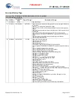
Document #: 001-45754 Rev. *B

Revised November 10, 2008

Page 24 of 24

AutoStore and QuantumTrap are registered trademarks of Simtek Corporation. All products and company names mentioned in this document are the trademarks of their respective holders.

PRELIMINARY

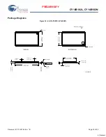
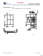
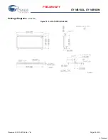
CY14B102L, CY14B102N

© Cypress Semiconductor Corporation, 2008. The information contained herein is subject to change without notice. Cypress Semiconductor Corporation assumes no responsibility for the use of any
circuitry other than circuitry embodied in a Cypress product. Nor does it convey or imply any license under patent or other rights. Cypress products are not warranted nor intended to be used for medical,
life support, life saving, critical control or safety applications, unless pursuant to an express written agreement with Cypress. Furthermore, Cypress does not authorize its products for use as critical
components in life-support systems where a malfunction or failure may reasonably be expected to result in significant injury to the user. The inclusion of Cypress products in life-support systems
application implies that the manufacturer assumes all risk of such use and in doing so indemnifies Cypress against all charges. 

Any Source Code (software and/or firmware) is owned by Cypress Semiconductor Corporation (Cypress) and is protected by and subject to worldwide patent protection (United States and foreign),
United States copyright laws and international treaty provisions. Cypress hereby grants to licensee a personal, non-exclusive, non-transferable license to copy, use, modify, create derivative works of,
and compile the Cypress Source Code and derivative works for the sole purpose of creating custom software and or firmware in support of licensee product to be used only in conjunction with a Cypress
integrated circuit as specified in the applicable agreement. Any reproduction, modification, translation, compilation, or representation of this Source Code except as specified above is prohibited without
the express written permission of Cypress. 

Disclaimer: CYPRESS MAKES NO WARRANTY OF ANY KIND, EXPRESS OR IMPLIED, WITH REGARD TO THIS MATERIAL, INCLUDING, BUT NOT LIMITED TO, THE IMPLIED WARRANTIES
OF MERCHANTABILITY AND FITNESS FOR A PARTICULAR PURPOSE. Cypress reserves the right to make changes without further notice to the materials described herein. Cypress does not
assume any liability arising out of the application or use of any product or circuit described herein. Cypress does not authorize its products for use as critical components in life-support systems where
a malfunction or failure may reasonably be expected to result in significant injury to the user. The inclusion of Cypress’ product in a life-support systems application implies that the manufacturer
assumes all risk of such use and in doing so indemnifies Cypress against all charges. 

Use may be limited by and subject to the applicable Cypress software license agreement. 

Sales, Solutions, and Legal Information

Worldwide Sales and Design Support

Cypress maintains a worldwide network of offices, solution centers, manufacturer’s representatives, and distributors. To find the office

closest to you, visit us at 

cypress.com/sales.

Products

PSoC

psoc.cypress.com

Clocks & Buffers

clocks.cypress.com

Wireless

wireless.cypress.com

Memories

memory.cypress.com

Image Sensors

image.cypress.com

PSoC Solutions

General

psoc.cypress.com/solutions

Low Power/Low Voltage

psoc.cypress.com/low-power


Precision Analog 

psoc.cypress.com/precision-analog

LCD Drive

psoc.cypress.com/lcd-drive

CAN 2.0b

psoc.cypress.com/can

USB

psoc.cypress.com/usb

[+] Feedback 

Summary of Contents for Perform CY14B102L

Page 1: ... a nonvolatile element in each memory cell The memory is organized as 256K bytes of 8 bits each or 128K words of 16 bits each The embedded nonvolatile elements incorporate QuantumTrap technology producing the world s most reliable nonvolatile memory The SRAM provides infinite read and write cycles while independent nonvolatile data resides in the highly reliable QuantumTrap cell Data transfers fro...

Page 2: ... 4 Mbit NC pin not connected to die 5 Address expansion for 8 Mbit NC pin not connected to die 6 Address expansion for 16 Mbit NC pin not connected to die 7 HSB pin is not available in 44 TSOP II x16 package 44 TSOP II x16 44 TSOP II x8 7 NC A8 NC NC VSS DQ6 DQ5 DQ4 VCC A13 DQ3 A12 DQ2 DQ1 DQ0 OE A9 CE NC A0 A1 A2 A3 A4 A5 A6 A11 A7 A14 A15 A16 A17 NC NC 1 2 3 4 5 6 7 8 9 10 11 12 13 14 15 16 17 1...

Page 3: ...ctive LOW Controls DQ15 DQ8 BLE Input Byte Low Enable Active LOW Controls DQ7 DQ0 VSS Ground Ground for the Device Must be connected to the ground of the system VCC Power Supply Power Supply Inputs to the Device HSB 7 Input Output Hardware Store Busy HSB When LOW this output indicates that a hardware store is in progress When pulled LOW external to the chip it initiates a nonvolatile STORE operati...

Page 4: ...ation is a unique feature of QuantumTrap technology and is enabled by default on the CY14B102L CY14B102N During a normal operation the device draws current from VCC to charge a capacitor connected to the VCAP pin This stored charge is used by the chip to perform a single STORE operation If the voltage on the VCC pin drops below VSWITCH the part automatically disconnects the VCAP pin from VCC A STO...

Page 5: ...B will be driven LOW It is important to use read cycles and not write cycles in the sequence although it is not necessary that OE be LOW for a valid sequence After the tSTORE cycle time is fulfilled the SRAM is activated again for the read and write operation Software RECALL Transfer the data from the nonvolatile memory to the SRAM with a software address sequence A software RECALL cycle is initia...

Page 6: ... must be issued to save the AutoStore state through subsequent power down cycles The part comes from the factory with AutoStore enabled Data Protection The CY14B102L CY14B102N protects data from corruption during low voltage conditions by inhibiting all externally initiated STORE and write operations The low voltage condition is detected when VCC VSWITCH If the CY14B102L CY14B102N is in a write mo...

Page 7: ...RC 25 ns tRC 45 ns Values obtained without output loads IOUT 0 mA Automotive 90 75 mA mA ICC2 Average VCC Current during STORE All Inputs Don t Care VCC Max Average current for duration tSTORE 10 mA ICC3 11 AverageVCC Currentat tRC 200 ns 3V 25 C typical All I P cycling at CMOS levels Values obtained without output loads IOUT 0 mA 35 mA ICC4 Average VCAP Current during AutoStore Cycle All Inputs D...

Page 8: ...ut Capacitance TA 25 C f 1 MHz VCC 0 to 3 0V 7 pF COUT Output Capacitance 7 pF Thermal Resistance In the following table the thermal resistance parameters are listed 14 Parameter Description Test Conditions 48 FBGA 44 TSOP II 54 TSOP II Unit ΘJA Thermal Resistance Junction to Ambient Test conditions follow standard test methods and procedures for measuring thermal impedance in accordance with EIA ...

Page 9: ...0 0 0 ns tHZBE Byte Disable to Output Inactive 8 10 15 ns SRAM Write Cycle tWC tWC Write Cycle Time 20 25 45 ns tPWE tWP Write Pulse Width 15 20 30 ns tSCE tCW Chip Enable To End of Write 15 20 30 ns tSD tDW Data Setup to End of Write 8 10 15 ns tHD tDH Data Hold After End of Write 0 0 0 ns tAW tAW Address Setup to End of Write 15 20 30 ns tSA tAS Address Setup to Start of Write 0 0 0 ns tHA tWR A...

Page 10: ...re 8 SRAM Write Cycle 1 WE Controlled 3 18 19 20 GGUHVV 9DOLG GGUHVV DWD 2XWSXW 2XWSXW DWD 9DOLG 6WDQGE FWLYH LJK PSHGDQFH 2 W W5 W W W W 2 W 2 W W W38 W3 W W 2 DWD 2XWSXW DWD QSXW QSXW DWD 9DOLG LJK PSHGDQFH GGUHVV 9DOLG GGUHVV 3UHYLRXV DWD W W6 W W W W3 W6 W6 W W W Notes 20 CE or WE must be VIH during address transitions Feedback ...

Page 11: ...ite Cycle 2 CE Controlled 3 18 19 20 Figure 10 SRAM Write Cycle 3 BHE and BLE Controlled 3 18 19 20 DWD 2XWSXW DWD QSXW QSXW DWD 9DOLG LJK PSHGDQFH GGUHVV 9DOLG GGUHVV W W6 W W6 W6 W W W W3 DWD 2XWSXW DWD QSXW QSXW DWD 9DOLG LJK PSHGDQFH GGUHVV 9DOLG GGUHVV W W6 W W6 W6 W W W W3 Feedback ...

Page 12: ...Waveforms Figure 11 AutoStore or Power Up RECALL 24 96 7 9 6 99 5 6 W6725 W6725 W W W W W 6 W 6 W 5 W 5 6 287 XWRVWRUH 32 5 83 5 5HDG ULWH QKLELWHG 5 32 5 83 5 5HDG ULWH 52 1 287 XWRVWRUH 32 5 83 5 5HDG ULWH 32 5 2 1 XWRVWRUH 1RWH 1RWH 1RWH Notes 21 tHRECALL starts from the time VCC rises above VSWITCH 22 If an SRAM write has not taken place since the last nonvolatile cycle no AutoStore or Hardwar...

Page 13: ...0 ns tHA Address Hold Time 0 0 0 ns tRECALL RECALL Duration 200 200 200 μs Switching Waveforms Figure 12 CE and OE Controlled Software STORE RECALL Cycle 27 Figure 13 Autostore Enable Disable Cycle W5 W5 W6 W W W6 W W W W W W W W6725 W5 W W 6 LJK PSHGDQFH GGUHVV GGUHVV GGUHVV 2 6 6725 RQO 4 7 5 W5 W5 W6 W W W6 W W W W W W W GGUHVV GGUHVV GGUHVV 2 4 7 5 W66 Notes 26 The software sequence is clocked...

Page 14: ...ing 28 29 W3 6 W3 6 W W 6 W W6725 W W 6 ULWH ODWFK VHW ULWH ODWFK QRW VHW 6 1 6 287 4 DWD 2XW 5 6 1 6 287 5 6 SLQ LV GULYHQ KLJK WR 9 RQO E QWHUQDO 65 0 LV GLVDEOHG DV ORQJ DV 6 1 LV GULYHQ ORZ 6 GULYHU LV GLVDEOHG W 6 N2KP UHVLVWRU GGUHVV GGUHVV GGUHVV GGUHVV 6RIW 6HTXHQFH RPPDQG W66 W66 GGUHVV 9 W6 W 6RIW 6HTXHQFH RPPDQG W Notes 28 This is the amount of time it takes to take action on a soft seq...

Page 15: ...n CE WE OE BHE BLE Inputs Outputs 2 Mode Power H X X X X High Z Deselect Power down Standby L X X H H High Z Output Disabled Active L H L L L Data Out DQ0 DQ15 Read Active L H L H L Data Out DQ0 DQ7 DQ8 DQ15 in High Z Read Active L H L L H Data Out DQ8 DQ15 DQ0 DQ7 in High Z Read Active L H H L L High Z Output Disabled Active L H H H L High Z Output Disabled Active L H H L H High Z Output Disabled...

Page 16: ...60 54 pin TSOP II Commercial CY14B102L ZSP20XIT 51 85160 54 pin TSOP II Industrial CY14B102L ZSP20XI 51 85160 54 pin TSOP II CY14B102L ZSP20XAT 51 85160 54 pin TSOP II Automotive CY14B102N ZS20XCT 51 85087 44 pin TSOP II Commercial CY14B102N ZS20XIT 51 85087 44 pin TSOP II Industrial CY14B102N ZS20XI 51 85087 44 pin TSOP II CY14B102N ZS20XAT 51 85087 44 pin TSOP II Automotive CY14B102N BA20XCT 51 ...

Page 17: ...P25XI 51 85160 54 pin TSOP II CY14B102L ZSP25XAT 51 85160 54 pin TSOP II Automotive CY14B102N ZS25XCT 51 85087 44 pin TSOP II Commercial CY14B102N ZS25XIT 51 85087 44 pin TSOP II Industrial CY14B102N ZS25XI 51 85087 44 pin TSOP II CY14B102N ZS25XAT 51 85087 44 pin TSOP II Automotive CY14B102N BA25XCT 51 85128 48 ball FBGA Commercial CY14B102N BA25XIT 51 85128 48 ball FBGA Industrial CY14B102N BA25...

Page 18: ...tive CY14B102N ZS45XCT 51 85087 44 pin TSOP II Commercial CY14B102N ZS45XIT 51 85087 44 pin TSOP II Industrial CY14B102N ZS45XI 51 85087 44 pin TSOP II CY14B102N ZS45XAT 51 85087 44 pin TSOP II Automotive CY14B102N BA45XCT 51 85128 48 ball FBGA Commercial CY14B102N BA45XIT 51 85128 48 ball FBGA Industrial CY14B102N BA45XI 51 85128 48 ball FBGA CY14B102N BA45XAT 51 85128 48 ball FBGA Automotive CY1...

Page 19: ...Std Speed 20 20ns 45 45 ns Data Bus L x8 N x16 Density 102 2 Mb Voltage B 3 0V Cypress CY 14 B 102 L ZS P 20 X C T NVSRAM 14 Auto Store Software Store Hardware Store Temperature C Commercial 0 to 70 C I Industrial 40 to 85 C Pb Free Package BA 48 FBGA ZS TSOP II P 54 Pin Blank 44 Pin A Automotive 40 to 125 C 25 25ns Feedback ...

Page 20: ...0 PLANE SEATING PIN 1 I D 44 1 18 517 0 729 0 800 BSC 0 5 0 400 0 016 0 300 0 012 EJECTOR PIN R G O K E A X S 11 735 0 462 10 058 0 396 10 262 0 404 1 194 0 047 0 991 0 039 0 150 0 0059 0 050 0 0020 0 0315 18 313 0 721 10 058 0 396 10 262 0 404 0 597 0 0235 0 406 0 0160 0 210 0 0083 0 120 0 0047 BASE PLANE 0 10 004 22 23 TOP VIEW BOTTOM VIEW 51 85087 A Feedback ...

Page 21: ...ge Diagrams continued A 1 A1 CORNER 0 75 0 75 Ø0 30 0 05 48X Ø0 25 M C A B Ø0 05 M C B A 0 15 4X 0 21 0 05 1 20 MAX C SEATING PLANE 0 53 0 05 0 25 C 0 15 C A1 CORNER TOP VIEW BOTTOM VIEW 2 3 4 3 75 5 25 B C D E F G H 6 5 4 6 5 2 3 1 D H F G E C B A 6 00 0 10 10 00 0 10 A 10 00 0 10 6 00 0 10 B 1 875 2 625 0 36 51 85128 D Feedback ...

Page 22: ...PRELIMINARY CY14B102L CY14B102N Document 001 45754 Rev B Page 22 of 24 Figure 18 54 Pin TSOP II 51 85160 Package Diagrams continued 51 85160 Feedback ...

Page 23: ...E HSB and NC pin description Page 4 Updated SRAM READ SRAM WRITE Autostore operation descrip tion Page 4 Updated Hardware store operation Page 5 Hardware RECALL Power up description Page 6 updated Data protection description Maximum Ratings Added Max Accumulated storage time Changed ICC2 from 6mA to 10mA Changed ICC4 from 6mA to 5mA Changed ISB from 3mA to 5mA Updated ICC1 ICC3 ISBand IOZ Test con...

Page 24: ...irmware in support of licensee product to be used only in conjunction with a Cypress integrated circuit as specified in the applicable agreement Any reproduction modification translation compilation or representation of this Source Code except as specified above is prohibited without the express written permission of Cypress Disclaimer CYPRESS MAKES NO WARRANTY OF ANY KIND EXPRESS OR IMPLIED WITH ...

Reviews: