320
CY8C28xxx PSoC Programmable System-on-Chip TRM, Document No. 001-52594 Rev. *G
Global Digital Interconnect (GDI)
14.1.3
44-Pin Global Interconnect
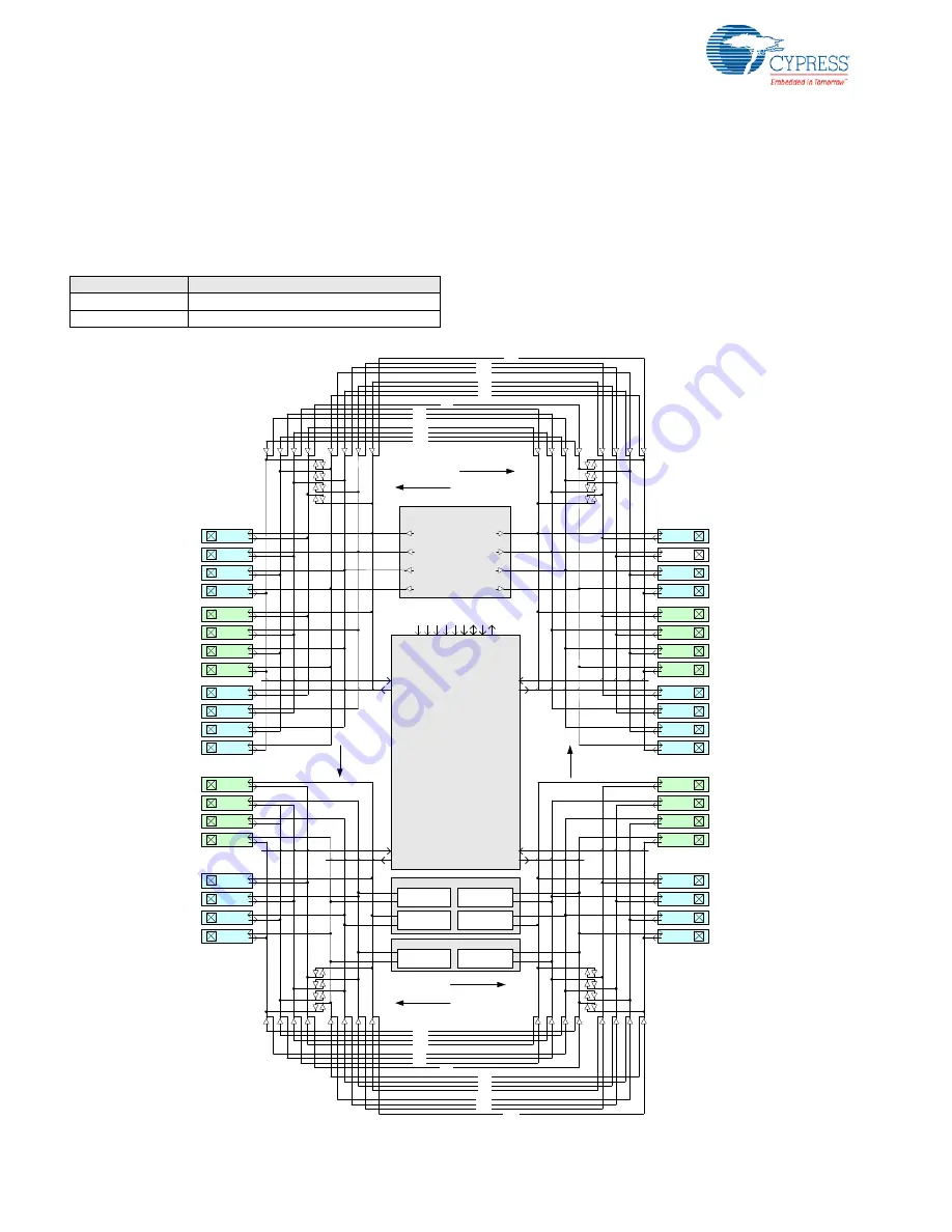
For 44-pin PSoC devices, there are five 8-bit ports. There-
fore, there are up to three ports connected to the even
global buses and two ports connected to the odd global
buses.
lists the mapping between global buses
and ports.
Because several ports are connected to a single global bus,
there is a one-to-many mapping between individual nets in a
global bus and port pins. For example, if GIO[1] is used to
bring an input signal into a digital PSoC block, either pin
P1[1] or P3[1] may be used. The same is true for the out-
puts. For example, if GOE[3] is used to carry a signal from a
digital PSoC block to a port pin, any or all of the following
pins may be used: P0[3], P2[3], or P4[3].
To determine the number of digital rows and digital blocks in
your PSoC device, refer to the table titled
.
Figure 14-3. Global Interconnect Block Diagram for the CY8C285xx 44-Pin Package
Table 14-2. 44-Pin Global Bus to Port Mapping
Global Bus
Ports
GIO[7:0], GOO[7:0]
P1, P3
GIE[7:0], GOE[7:0]
P0, P2, P4
P0[6]
GO
GI
P0[4]
GO
GI
P0[2]
GO
GI
P0[7]
GO
GI
P0[5]
GO
GI
P0[3]
GO
GI
P0[1]
GO
GI
P0[0]
GO
GI
P2[6]
GO
GI
P2[4]
GO
GI
P2[2]
GO
GI
P2[7]
GO
GI
P2[5]
GO
GI
P2[3]
GO
GI
P2[1]
GO
GI
P2[0]
GO
GI
P4[4]
GO
GI
P4[2]
GO
GI
P4[5]
GO
GI
P4[3]
GO
GI
P4[1]
GO
GI
P4[0]
GO
GI
P3[6]
GO
GI
P3[4]
GO
GI
P3[2]
GO
GI
P3[7]
GO
GI
P3[5]
GO
GI
P3[3]
GO
GI
P3[1]
GO
GI
P3[0]
GO
GI
P1[6]
GO
GI
P1[4]
GO
GI
P1[2]
GO
GI
P1[7]
GO
GI
P1[5]
GO
GI
P1[3]
GO
GI
P1[1]
GO
GI
P1[0]
GO
GI
GI
E[
0]
GI
E[
2]
GI
E[
4]
GI
E[
6]
GO
E[
0]
GO
E[
2]
GO
E[
4]
GO
E[
6]
GOE[7]
GOE[5]
GOE[3]
GOE[1]
GI
E[
7]
GI
E[
5]
GI
E[
3]
GI
E[
1]
GIO[0]
GIO[2]
GIO[4]
GIO[6]
G
OO[0
]
G
OO[2
]
G
OO[4
]
G
OO[6
]
GO
O[7
]
GO
O[5
]
GO
O[3
]
GO
O[1
]
GI
O[7
]
GI
O[5
]
GI
O[3
]
GI
O[1
]
Even Numbered Pins
Odd Numbered Pins
GIO[7,5,3,1]
GIE[7,5,3,1]
D
B[7
:0
]
DB
I
IN
T[
23
:8
]
CL
K3
2K
VC
3
ACMP[3
:0
]
SY
SC
LK
X2
VC
2
VC
1
GIO[6,4,2,0]
GIE[6,4,2,0]
GOO[7,5,3,1]
GOE[7,5,3,1]
GOO[6,4,2,0]
GOE[6,4,2,0]
Digital PSoC Array
SYSCLKX2
SYSCLK
CLK32K
Digital Clocks
VC3
VC1
VC2
Odd
Numbered
Ports
Even
Numbered
Ports
SLPINT
CLK24M
Even Numbered Pins
Odd Numbered Pins
GOO[0]
GOO[2]
GOO[4]
GOO[6]
GIO[1]
GIO[3]
GIO[5]
GIO[7]
GIO[0]
GIO[2]
GIO[4]
GIO[6]
GOO[1]
GOO[3]
GOO[5]
GOO[7]
GOE[0]
GOE[2]
GOE[4]
GOE[6]
GIE[1]
GIE[3]
GIE[5]
GIE[7]
GIE[0]
GIE[2]
GIE[4]
GIE[6]
GOE[1]
GOE[3]
GOE[5]
GOE[7]
CY8C28xxx Type-E Column
AEC1
AEC0
CY8C28xxx Analog Array
ACC Comp
Bus 1
ACC Comp
Bus 0
ACC Comp
Bus 3
ACC Comp
Bus 2
P4[7]
GO
GI
P4[6]
GO
GI
Summary of Contents for CY8C28 series
Page 65: ...64 CY8C28xxx PSoC Programmable System on Chip TRM Document No 001 52594 Rev G RAM Paging ...
Page 125: ...124 CY8C28xxx PSoC Programmable System on Chip TRM Document No 001 52594 Rev G ...
Page 311: ...310 CY8C28xxx PSoC Programmable System on Chip TRM Document No 001 52594 Rev G IDAC_CR0 1 FDh ...
Page 317: ...316 CY8C28xxx PSoC Programmable System on Chip TRM Document No 001 52594 Rev G ...
Page 393: ...392 CY8C28xxx PSoC Programmable System on Chip TRM Document No 001 52594 Rev G ...
Page 477: ...476 CY8C28xxx PSoC Programmable System on Chip TRM Document No 001 52594 Rev G Digital Clocks ...
Page 561: ...560 CY8C28xxx PSoC Programmable System on Chip TRM Document No 001 52594 Rev G ...


