PSoC Analog Coprocessor Pioneer Kit Guide, Doc. # 002-11190 Rev. *B
46
A.3.3
Write/Read Operation
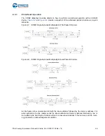
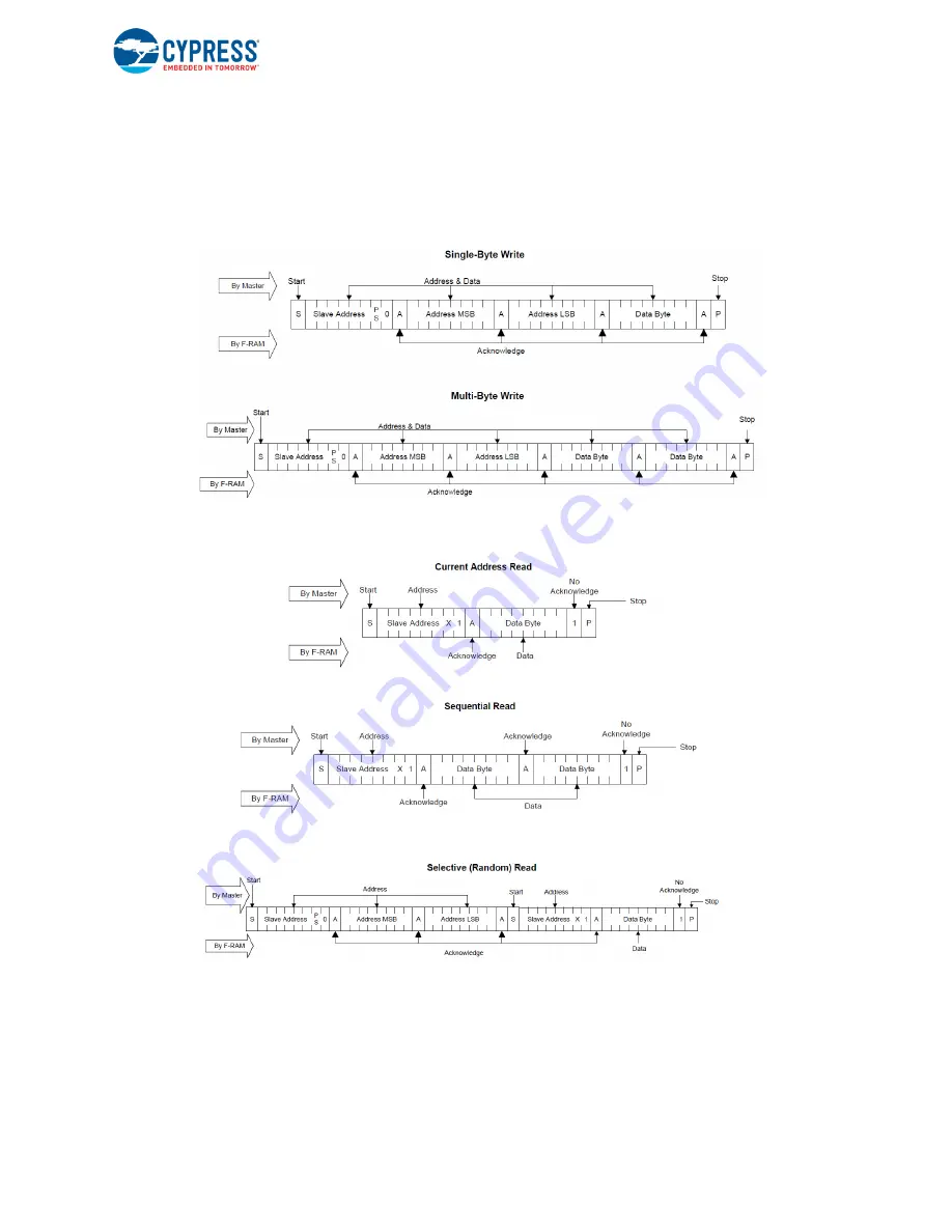
The F-RAM datasheet includes details on how to perform a write/read operation with an F-RAM
device.
and
provide a snapshot of the write/read packet structure as a quick
reference.
Figure A-7. F-RAM Single-Byte and Multiple-Byte Write Packet Structure
Figure A-8. F-RAM Single-Byte and Multiple-Byte Read Packet Structure
As the figures show, operations start with the slave address followed by the memory address. For
write operations, the bus master sends the slave address and memory address followed by one or
more data bytes. Each byte of data is written to consecutive locations in the memory, and the mem-
ory generates an acknowledgement condition.


