EE Pro for TI - 89, 92 Plus
Equations - OpAmp Circuits
69
Rs
Voltage divide resistor
Ω
tr
10-90% rise time
s
∆
VH
Hysteresis
V
VL
Detection threshold, low
V
Vomax
Maximum circuit output
V
VR
Reference voltage
V
Vrate
Maximum voltage rate
V/s
VU
Detection threshold, high
V
Vz1
Zener breakdown 1
V
Vz2
Zener breakdown 2
V
26.1 Basic Inverter
These equations define the properties of a basic inverter. The first equation relates the
voltage gain Av to the feedback resistance Rf and input resistance RR1. The optimum
value of Rp is defined by the second equation to minimize output-voltage offset due to
input bias current. The first pole frequency fcp is defined by the third equation. Small
signal rise time tr (10 to 90%) is defined by the fourth equation.
Av
Rf
RR
= −
1
Eq. 26.1.1
Rp
RR
Rf
RR
Rf
=
⋅
+
1
1
Eq. 26.1.2
fcp
fop
Av
RR
Rf
=
⋅ −
⋅
F
HG
I
KJ
(
)
1
Eq. 26.1.3
tr
Rf
fop
Av
RR
=
⋅
⋅ −
⋅
.
(
)
35
1
Eq. 26.1.4
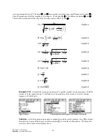
Example 26.1 -
Find the gain of an inverter and its optimum value for bias resistance given an input resistance
of 1 k
Ω
and a feedback resistance of 20 k
Ω
.
Entered Values
Calculated Results
Solution -
Use the first and second equations to compute the solution for this problem. Select these by
highlighting each equation and pressing the
¸
key. Press
„
to display the input screen, enter all the known
variables and press
„
to solve the equation. The computed results are shown in the screen displays above.
-PQYP8CTKCDNGU44
AM
Ω
, Rf=20._k
Ω
%QORWVGF4GUWNVU
#X
4R
A
Ω


