EE PRO for TI-89, 92 Plus
Equations - Solid State Devices
89
IB
q A DE
LE
nE
e
q A
DC
LC
nnC e
q VBE
k TT
q VCB
k TT
= ⋅ ⋅
⋅
⋅
−
F
HG
I
KJ
+ ⋅
⋅
⋅
−
F
HG
I
KJ
⋅
⋅
⋅
⋅
1
1
2
1
Eq. 27.6.3
α =
⋅
⋅
+
⋅
DB pB
WB
DB pB
WB
DE nE
LE
Eq. 27.6.4
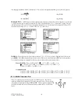
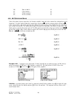
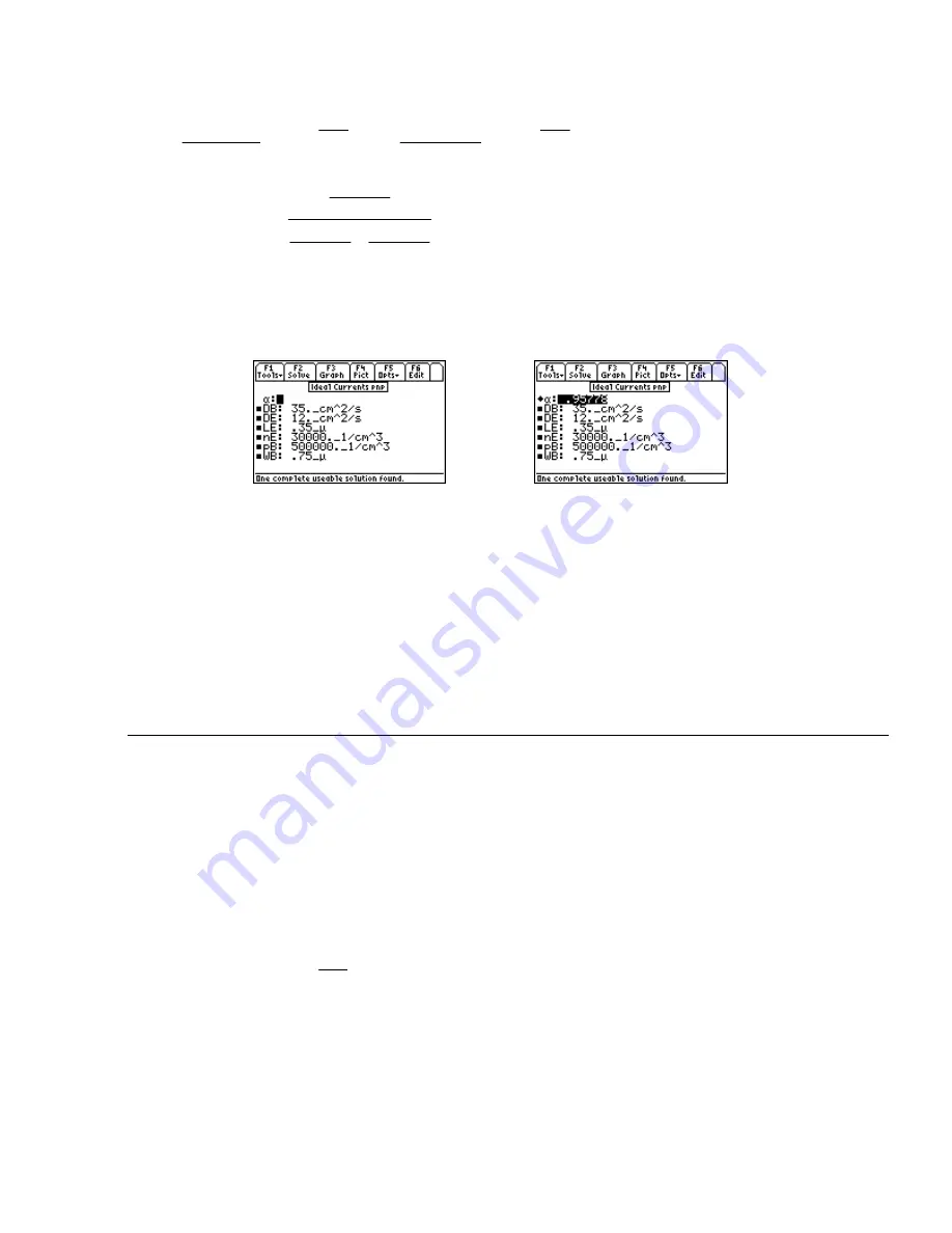
Example 27.6 -
Find the emitter current gain
α
for a transistor with the following properties: base width of 0.75
µ
m, base diffusion coefficient of 35 cm
2
/s, emitter diffusion coefficient of 12 cm
2
/s, and emitter diffusion length of
0.35
µ
m. The emitter electron density is 30,000 cm
-3
and the base density is 500,000 cm
-3
.
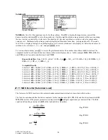
Entered Values
Calculated Results
Solution -
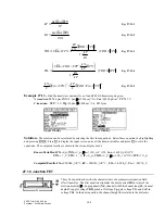
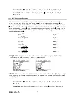
Use the last equation to compute the solution for this problem. Select this by highlighting each equation
and pressing the
¸
key. Press
„
to display the input screen, enter all the known variables and press
„
to solve
the equation. The computed results are shown in the screen displays above.
-PQYP8CTKCDNGU&$
AEO@U
&'
EO@U
.'
A
µ
P'
AEO@
R$
AEO@
9$
A
µ
%QORWVGF4GUWNVU
αα
27.7 Switching Transients
These six equations compute the key relationships in determining switching response times of bipolar transistors. The
work of Ebers and Moll was supplemented by Gummel to model transistor behavior in several different ways. The
concept of charge in the base of the transistor controlling switching times became an important contribution to
switching theory.
The first equation expresses the base charge at the edge of saturation Qsat in terms of the collector saturation current
ICsat and the base transit time
ττ
t. The collector saturation is determined (approximately) by the second equation in
terms of supply voltage VCC and load resistance Rl.
Qsat
ICsat
t
=
⋅
τ
Eq. 27.7.1
ICsat
Vcc
Rl
=
Eq. 27.7.2
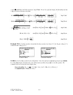
The third equation calculates the turn-on transient time tr in terms of base recombination time
ττ
B, ICsat, base current
IB and base transit time
ττ
t. The fourth equation computes the storage delay tsd1 when the bipolar transistor is
switched from the saturation region to cutoff by changing the base current from IB to 0. The penultimate equation
shows the storage delay tsd2 when the base current is switched from IB to -IB. The final equation computes the so
called saturation voltage VCEs, the voltage drop between the collector and the emitter under full saturation, in terms of
the collector and base currents IC and IB and the forward and reverse
α
’s
αα
f and
αα
r.


